Wireless Powers - Backwards Engeneering Electric Toothbrush

Hi Everyone

I am interested to learn more about wireless power, and decided to break open a generic electric toothbrush, to find out how it works. (There was a moment of irony when the lady called me back saying "Sir, you forgot your receipt, you need this otherwise our warranty does not cover your purchase")

Anyway.
So I am going to document the process here, and If anyone wants to pitch in, give feedback on the way, that would be cool.

So these are the guts.

The toothbrush part is simple enough. There is a zener diode for voltage regulation, Ni-Mh battery at 1.2V, a regular DC motor and some gear which convert the rotary movement to an oscillatory movement.

The charging circuit is a bit more complex though:

I'm trying to figure out what exactly is happening here. I thought that all I would find here would be some voltage regulation circuit, i.e. two coupled zener diodes and some resistors.

So, I did some photoshopping (well, actually I used Gimp, which I dont know how to use, so the results are mediocre... but here goes:)

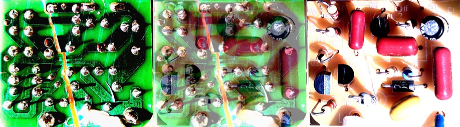
So, what parts are there?

(using the pcb's markings)

6 regular resistors

R2 = 43k Ohm (5%)
R4 = 3.3k Ohm (5%)
R5 = 820 Ohm (5%)
R6 = 1.8k Ohm (5%)
R7 = 51 Ohm (5%)

R9 = 82k Ohm (5%)

1 blue resistor
R3 = 13.6M Ohm (0.05%)

1 big light blue resistor (R8)
R8 = F1/2J D5K 820 Ohm

3 Transistors
Q1 = MPSA 44 G8 C
Q2 = BC 547B G5 E
Q3 = BC 547B G5 E

1 Diode
D1 = (400 013)? (cant read it propperly)

3 Dark Brown Squarish Ceramic Caps:
C2 = CL21 682 k 400
C3 = CL21 154 K 250
C4 = 333JA 400

1 Light brown Roundish Ceramic Cap (?) or big ass Resistor?:
R1 = TVR 07471 (is this a resistor array? is it mislabelled?)

1 Electrolytic Capacitor

C1 = KM(M) Z 6 A 105° C8

So, some of these parts I vaguely understand, some I have no clue what they do.

Can anyone shed some light in this? In theory all this circuit should be doing is drop the voltage to safe levels and then (while maintinging the AC signal) power the coil. I guess some of the resistors are required to keep the current down and not burn out the whole thing... maybe thats what R1 is for?)

I have to do some stuff for university, but I plan on eventually drawing a schematic to help me understand this. Can anyone recommend some software for the schematic? Fritzing does not appeal to me that much, and eagle is too complicated for what I want to do... anything simple out there?

Anyway, I will continue on this later. Any input you can give me would be appreceated

Cheers

p.

Interesting project. I'm afraid I can't help you out but I'll read updates :smiley:
Best regards
Jantje

Is there perhaps something there to create a higher frequency in the coil to improve the charging over if they used mains frequency only? Like Jantje, I don't know but am keen to read what you learn, Geoff

The TVR 07471 is a transient voltage supressor
http://www.aeontekasia.com/pdf/TVR.pdf

if all else fails google it LOL

what i think is happening here is based on my alevel physics so i may not be correct but what i think is here the base holds the primary coil for a transformer and that when the toothbrush is entered into the centre coil it acts as the secondary coil but this would "wirelessly" transfer voltage via electromagnetism to create a voltage and current in the secondary coil.

a capacitor can be used to create a phase difference between the input and output
[this is an all pass filter featuring an op-amp this may look like a certain circuit above?]

Wikipedia:
An all-pass filter is a signal processing filter that passes all frequencies equally, but changes the phase relationship between various frequencies. It does this by varying its propagation delay with frequency. Generally, the filter is described by the frequency at which the phase shift crosses 90° (i.e., when the input and output signals go into quadrature — when there is a quarter wavelength of delay between them).

so the wireless charging capabilities comes from the AC transformer of primary and secondary coils

just my take on it and it could well be totally wrong but anyone who does know for sure id be happy find out whether im correct or not

Ok, so I tried to draw a schematic:

(please understand, I have no formal training in electronics what-so-ever, so I may be ignoring many standard conventions here - if you have suggestions on how to improve this, please don't hesitate to point them out to me.)

@Jantja & strykeroz

Thanks for the interest :slight_smile:

@KG4MXV

Thanks for googling :slight_smile:

@ocmurf

yep thats basically whats happening (ad. transformer)
however: how does the all-pass filter fit in? How would phase shifting influence the behavior of the coils? As far as I understand, its the oscillation of the voltage in the primary coil/ the rapid change in magnetic field which induce electricity in the secondary coil. Phase shifting would merely act as offset, no?

Also, there is no op-amp in the circuit (or am I missing something obious?)

The Transient Voltage Suppressor (I am just gonna pretend its a diode. I don't really get what it does yet, completely) is arbitrarily placed - i am using the diode symbol to represent it, which might not really be appropriated.

I guess R8, D1 (accidentally marked it as D2 in the schematic) C4 & TVR 0747 together make up some type of voltage regulation circuit.

Between Q1, Q2, Q3 there seems to be some type of feedback thing going on. Would this maybe be increasing the oscillation frequency like strykeroz suggested?

The schematic is now arranged very closely to how things are physically arranged - if anyone has suggestions on how to arrange the parts so they are easyer to understand that would be awesome.

Also if anyone who knows more about these things than I do could point out some of the things which might be going on there, that would be amazing.

Cheers

p.

simple google search brings up this on wikipedia about the transistant voltage suppressor :

wikipedia:
A transient-voltage-suppression (TVS) diode is an electronic component used to protect sensitive electronics from voltage spikes induced on connected wires.[1] The device operates by shunting excess current when the induced voltage exceeds the avalanche breakdown potential. It is a clamping device, suppressing all overvoltages above its breakdown voltage. Like all clamping devices, it automatically resets when the overvoltage goes away

Source:Transient-voltage-suppression diode - Wikipedia

so basically it seems that the diode does not allow the circuit to have above a certain limit flowing through it this is probably to stop the battery being charged incorrectly again this is my understanding i may be wrong

I'm not going by the circuit, I am just thinking out loud... does the circuit act as a regulator, with the amount of power being allowed through the primary being controlled by some sort of feedback? I'm just thinking if designing something like that, maybe it's designed to deliver charging power based upon the presence of a secondary in the field of the primary..