My project requires the use of a pair of cascaded 595 shift registers. And I need to consider the method that features least power consumption and also runs the fastest. Speed is marginally preferable to power efficiency in my case...
So my first port of call is the ShiftOut() documentation, which is great, but then that links me, tantalisingly(!) to the SPI library pages.
It says that the SPI library uses "hardware" rather than software. How exciting I thought, however sadly that's where the description stops. It does not suggest whether or not SPI is more or less efficient because it uses hardware. The curious reader is left nonplussed and uncertain as to which course of action to commit to.
Also the examples are uneven. Sure shiftout() has very good example code and also some (very) low resolution circuit diagrams but there is nothing comparable on the SPI side. Can we have an SPI example that drives a pair of shift registers like the ShiftOut() examples do?
Also, in the SPI docs, the concept of "Slave Select" is not clear. That needs to be explained in detail with an example (perhaps an arduino talking to 2 separate (non cascading) shift registers).
Phrasing: "Typically there are three lines common to all the devices..." - this then goes on to name 4 items, not 3. Is the last item not applicable?
The pin usage differences between the ShiftOut examples and the SPI examples are not adequately explained.
Rob,
I think you would still need the SS pin to act as the latch (or clock) for the output stage of the shift registers.
If you had multiple non-cascaded shift registers than each would need its own SS pin (assuming they share the clock & data pins).
One would assume that similar to hardware RX/TX being faster than Soft(ware) Serial, SPI would be similarly faster than Software Shiftout.
With the exception of needing to handle the SS in software still:
  // start up SPI to talk to the MAX7221
  SPI.begin(); // nothing in () because we are the master
  pinMode(SS, OUTPUT);  // Slave Select for SPI  <--- Need this here before any SPI writes?

  //  MAX7221: write shutdown register
  digitalWrite(SS,LOW);  // take the SS pin low to select the chip:
  SPI.transfer(SHUTDOWN_ADDRESS);  // select the Address,
  SPI.transfer(0x00);      // select the data, 0x00 = Outputs turned off
  digitalWrite(SS,HIGH);   // take the SS pin high to de-select the chip:
thus I could see replacing shiftout with this for sending 1 byte to a shift register
  SPI.transfer(your_data);  // shift out the 1 byte
  digitalWrite(SS,LOW);  // take the RCK pin lo/ho to move the data to the output register
  digitalWrite(SS,HIGH);   // in a 74HC595 or TPIC6B595 for example
Graynomad:
There is no obvious benefit to seperating the SRs though and it causes other issues, do you have a good reason to do so?
Rob
Well, that example is actually from a circuit where I had two displays both driven by a separate shift register, they both have to be driven very fast but never both at the same time. I'd be writing to one or the other at any given moment, but each only requires 8 bits of output. If you really must know it was a pie in the sky idea for a 3D heads up display, driven by an arduino. I think it's technically possible but at the moment is waaaay beyond my technical skill level. The design is flawed actually and needs a re-think before serious consideration is applied to actually building it.
"Typically there are three lines common to all the devices..." - this then goes on to name 4 items, not 3. Is the last item not applicable?
There are 4 wires used, but three of them are common to all devices, then each separate device needs it's own enable pin (unless it uses internal addressing like the 23S17)
Well, it's very clear that there are several people knowledgable on this subject - could we perhaps collaborate and get a nice bit of code and a circuit diagram together that shows idiots like me how to drive one 595 shift register using SPI.h functions? Then we can add quite a bit of value to the online docs by adding something that actually makes sense
I can drive a single SR using the "less efficient" ShiftOut() functionality (because it's docs very sensibly give actual pin numbers for BOTH Arduino and the 595) - but I'm having some real problems making the same thing happen using SPI.h. It's just not clear which arduino pin should be connected to the SR, the information assumes too much prior-knowledge in the reader. Simple and clear instructions get the project finished faster. The sooner people can get a project running the more enjoyment they derive from achieving something!
Enjoyment is the main point of Arduino right?
Then, once that is done, we can explain that the system can be extended by adding a second (third, fourth...) SR by chaining them together, the circuitry changes are already detailed in the ShiftOut() page.
I'll volunteer for guinea pig duty - send some code and a circuit diagram my way and I'll hook up my Uno and see if we can come up with some explanatory text to make it moron proof, this moron will work for free
I need this SPI/dual shift register stuff for my own project so I'll figure it out and try to document it with pinouts and perhaps a photo or two. Maybe others will have a use for it.
A good starting reference for SPI theory and usage is the AVR datasheet manual for the 328 processor.
Section 18 covers the topic well and even gives classic assembly and C coding examples.
A noobie question: on the right-hand circuit - the separate "out clock (Slave Selects)" lets you latch any single Shift Register of the three, independantly of the other two? In what situation would you use this functionality? Does the SS pin affect both the shifting-in of data AND latching or just latching?
CrossRoads:
What will you hook up to the outputs to show the blinding speed we'l achieve?
192 high candela blue LEDs, running at a rate of about 40 frames per second (something near 7800 * 16 shifted bits per second). It's not all that fast, but it will probably give you a headache if you stare at it for too long.
Does the SS pin affect both the shifting-in of data AND latching or just latching?
The SS pin is used to latch data on the output register when shifting out, and to latch data into the incoming parallel latch when shifting in.
This will need to be confirmed with a specific shift in register.
I only showed the two examples to show that more pins would be used for multiple independent parts. All would get the same data shifted in, but only 1 would have its data shifted into the output stage.
#include <SPI.h>
// SPI library sets up pins 11, 12, 13
int SS1 = 10;  // need for SPI
byte register1 = 0;
byte register2 = 0;
byte register3 = 0;
byye pinPWM = 3;

void setup() // stuff that runs once before looping forever
{
  // start up SPI to talk to the MAX7221
  SPI.begin(); // nothing in () because we are the master
  pinMode(SS1, OUTPUT);  // Slave Select for SPI  <--- Need this here before any SPI writes

  //  write out the data
  SPI.transfer(register1);  // 1st byte
  SPI.transfer(register2);  // 2nd byte
  SPI.transfer(register3);  // 3rd byte
  digitalWrite(SS1,LOW);  // take the SS pin low,
  digitalWrite(SS1,HIGH);   // take the SS pin high to latch data into output register
}

void loop (){
  // tricky part - making it do something

}
Crossroads: I tried the first of your two diagrams and it looks like it works fine, but I'm unsure about why you've connected PWM1 (Pin3 according to your code sample) to the SR. I've tried setting it high or low at various times but it doesn't seem to do anything, as soon as I set SS high and then low again the bits get pushed onto the outputs (and my LEDs light up). So basically I can control both chained SRs just using 3 pins on the arduino...
My pinout:
ARDUINO UNO Pin 13 (SPI:SCK)                    --->  74HC595 Pin 11 (SCK "Shift register clock input")
ARDUINO UNO Pin 11 (SPI:MOSI)                   --->  74HC595 Pin 14 (SER "Serial Data Input")
ARDUINO UNO Pin 10 (generic digital output)     --->  74HC595 Pin 12 (RCK "Storage register clock input")
ARDUINO UNO Pin GND                             ---> provides sink for circuit's GND rail
ARDUINO UNO Pin 5V                              ---> provides source for circuit's +5V rail
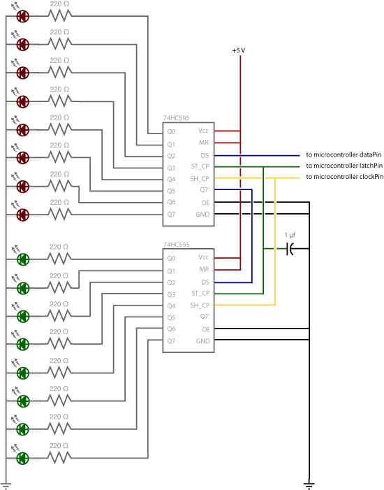
For the diagram I just used the one from the ShiftOut tutorial that uses 2 shift registers...
My code (flashes each of the 16 LEDs in turn)...
#include <SPI.h>

#define SHIFT_REGISTER_LATCH_SS (10)

void setup()
{
  //initialize SPI:
  SPI.setBitOrder(LSBFIRST);
  SPI.begin();
  pinMode(SHIFT_REGISTER_LATCH_SS, OUTPUT);

  //clear both shift registers so that all output pins go low
  SPI.transfer(0x00);
  SPI.transfer(0x00);
  digitalWrite(SHIFT_REGISTER_LATCH_SS, LOW);
  digitalWrite(SHIFT_REGISTER_LATCH_SS, HIGH);

  for (unsigned short int level = 1 ; level < 0x10000 ; level <<= 1)
  {
    UpdateDisplayPinFlags( (level >> 8) & 0xff, level & 0xff);
    delay(100);
  }

  UpdateDisplayPinFlags(0, 0);
}

void loop()
{
}

int UpdateDisplayPinFlags(byte high, byte low)
{
  SPI.transfer(low);
  SPI.transfer(high);
  digitalWrite(SHIFT_REGISTER_LATCH_SS, LOW);
  digitalWrite(SHIFT_REGISTER_LATCH_SS, HIGH);
}
This seems to work nicely (Although the code needs tidying up and commenting a bit) but there is always about 1 second where the first shift register (connected directly to the arduino) has a few bits high at startup. This happens before my code to zero them out executes. I can't seem to stop this in code. I've double checked my wiring against the diagram and I don't think I've missed anything. Any ideas?
The OEs on both chips are wired directly to GND as per the schematic. With regard to fading the LEDs, I think that's venturing outside the remit of the article we're trying to clarify. I think we should keep it simple for now.
Another problem I found with that original ShiftOut article is that it says use a 0.1"f capacitor between the latch pin (SS in this case) and GND. However the schematic says a 1µf. This is something we need to clarify also. Personally I've tried both and neither type make any apparent useful difference. The 1µf one actually prevents anything from being displayed on the output pins!
With OE tied to ground, whatever is in the output register will show up at the output at power on.
Maybe an RC circuit and a transistor to take it high on power up, and go low as the cap charges up & turns the transisto on.
I can't fathom why there would be an capacitor on the SS pin that would just degrade the signal.
original ShiftOut article is that it says use a 0.1"f capacitor between the latch pin (SS in this case) and GND
That's a known error and has been there forever. Why it isn't fixed is one of those great mysteries in life as it trips over evey newbie doing their first shift register project.
To be blunt, might it be such a bad idea if the entire set of reference pages was torn up and redone from scratch by those people who have the proper time to spend on good quality documentation? It seems that it was initially written by several over-excited hackers in a rush to build their next project and skimming over the details in order to get in more soldering time Can't say I blame them, I'd rather be building circuits than writing about how to do it.