While designing custom PCB's I always struggle setting the right decoupling capacitors. Sometimes, you can find requirements of the chip in its datasheet (e.g. the FT232RS, which requires a 100nf, a 10nf and a 4.7uf). But there are also times when there are probably "general" capacitors needed behind the power supply or nothing is stated in the datasheet.
Are there any rules of thumb? Like "every chip needs a 100nF as close as possible", or something like this?
That's 0.1uF per chip. Right next to the Vcc pin, like 0.1" to 0.2" away.
At the power supply itself, I go with 10uF on the input & 1uF on the output.
If using a wallwart for power, then just 10uF where it comes in the board.
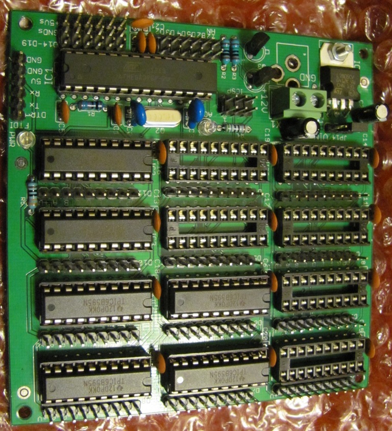
You can see the caps right next to the uC and shift register chips on this board. That's how close.
I sell caps or a living; unfortunately, rules of thumb only go so far. Depending on what the chip is doing, how the PCB is laid out, and the ability of the power supply, decoupling requirements will vary.
100nF and 10nF near the VCC of a chip is almost always a good idea. But you must keep in mind what that "chip" is.
Larger bulk values might be useful at the input of a board that is connected with a long cable ( like the 2 47uF near the barrel jacks of the Arduino board.)
Sometimes you need to make measurement or test the system to see what the rails look like.
There isn't a clear cut answer, except that not using them is a bad idea.
Are there any rules of thumb? Like "every chip needs a 100nF as close as possible", or something like this?
unless you will find such rules of thumb. That, by itself, is telling.
No. Digital devices are incredibly resistant to noises, including supply ripples, unlike analog devices. You can take a look at many digital devices - a motherboard, or a phone, if you need any confirmation of that.
Having said that, my approach to this is this:
a) decoupling for digital devices are not always necessary: for reasons I outlined earlier. I don't recall in my years of any digital circuit that didn't work because of lack of decoupling.
b) supply decoupling is generally a good practice, even for digital circuitry: one of the basic assumptions of a working circuit is a stable supply rail. It helps, however marginally, to ensure that that remains the case.
Never hurts to plan for a capacitor then leave the spot empty when you build the board. It hurts a lot more to not have a spot to add the capacitor when you need it.
GoingForGold:
And what would you consider as "close" to the chip? Is 1in of wire/copper still "close"?
As close as possible means "as close as possible". And with wide (low-inductance) traces. Really fast ICs
(100MHz + clocking) need decoupling within 1 to 2 mm of each and every supply pin and a groundplane
is essential... These chips switch in fractions of a nanosecond and every tiny scrap of stray inductance
counts.
Somewhat slower logic like the Arduino I'd say 5mm--10mm is worth aiming for and ground plane or grid is really
desirable. Unless you have the test equipment to measure the true nano-second timescale dips on the
supply and ground caused by switching transients you cannot tell how much slack you have, so you decouple
conservatively to avoid nasty surprises.
The basic rule is the faster the logic the smaller the decoupling capacitor is needed, but it must
be closer to the actual silicon (and usually more than one). The more current is switched the larger
the decoupling capacitor should be (or it should be split into a range of values with the smaller valued
ones closer to the chip).
Its hard to know the actual switched currents though, mostly these currents charge capacitances of
other MOSFETs on the chip and last for a few ns. You can get an estimate by looking at the current
consumption of a chip at its highest rated clockspeed - but that doesn't mean you need less decouplnig
if clocking at lower rates, since the switching transients are equally fast however seldom they happen.
Bypass/Decoupling caps are needed due to the parasitic inductance and resistance inherent in wiring and PCB traces, inductance limits how fast current can change. When working with high frequency digital ICs, current must be able to change quickly. Adding the bypass/decoupling capacitors as close as possible to the IC's V+ and GND pins effectively reduces the input impedance of the power supply + wiring.
You could also think of the bypass caps as tiny batteries that supply the IC with power until the power supply current can arrive to both fill the capacitor again and power the IC. The capacitor also passes any high frequency noise FROM the IC to ground, preventing interference.
Multiple value capacitors are used to cover multiple frequency requirements, or to have as low as possible ESR and ESL in the capacitance. MLCC (Mono/Ceramic) capacitors have extremely low ESR/ESL, but are also only mid capacity, they are the most common type of 0.1uF capacitors used for bypass. These are put in parallel with an electrolytic, which can filter the lower frequencies, but has higher ESR and ESL. When using an electrolytic, when the capacitors ESL/ESR is greater than that of the supplying circuit, their value cancels itself out in the best case, and they make things stop working in the worse case (see "capacitor plague").
All of the above is covered in the link below, but I thought I'd give a Cliff's notes in easier to understand language. Capacitor Design Data, and Decoupling Placement, How-To -This page covers everything you need to know, from layout and how bypass/decoupling capacitors work
There is an interesting bypassing technique used for driving PWM'd mosfet gates and that is to use a 220-680R resistor in series with the gate. When the controller brings the pin controlling the mosfet gate high (only where the gate is controlled directly by the controller) there is a very short surge current drawn by the gate capacitor as it is being charged to Vcc. The 220 - 680R resistor limits the current slightly and eliminates the resultant current spike to Vcc thus lowering overall supply noise. Supply noise isn't an issue for digital logic. However when Vcc noise becomes large enough, It will make logic circuitry like a controller unstable as it (the noise) can cause the controller to change states. Vcc noise with ANY type of analog measurement or processing simply isn't reliable... For example it is the most common source of random errors in making analog measurements. If a noise spike happens at the exact time that the measurement is done them the spike is included in the measurement returned.
Interesting discussion here. Can someone explain this one (from the XBee ZB product manual)? 8.2pF seems awfully small for a bypass capacitor. I'd designed several boards with XBees before I read this, using the "standard" 100nF (MLCC) bypass, without problems. Since I read this I've been installing 10uF MLCCs instead. Can't say I've ever seen an XBee bypassed according to this recommendation, which of course doesn't mean it's not a good idea!
Poor power supply can lead to poor radio performance especially if the supply voltage is not kept within
tolerance or is excessively noisy. To help reduce noise a 1uF and 8.2pF capacitor are recommended to be
placed as near to pin1 on the PCB as possible. If using a switching regulator for your power supply, switching
frequencies above 500kHz are preferred. Power supply ripple should be limited to a maximum 250mV peak to
peak.
For example, i'm using a load of 4000 logic IC's and simply by connecting positive/gnd every circuit, works, even 4017 but.... they're all very low speeds > 1hz and never had an issue and I always wondered why cap's were so important, take the attiny85, with no capacitor, it runs....
But an attiny85 at 8mhz, is not exactly high speed switching either....
So how fast we talking before a capacitor has to be sitting next to it?.... there has to be some guidelines?
I think the 8.2pF must be a misprint. A capacitor of that value isn't going to do anything useful by way of decoupling, especially given the distance between the Vcc and ground pins of that device. My guess is that they meant 8.2uF tantalum electrolytic, and ceramic for the other capacitor (1uF).