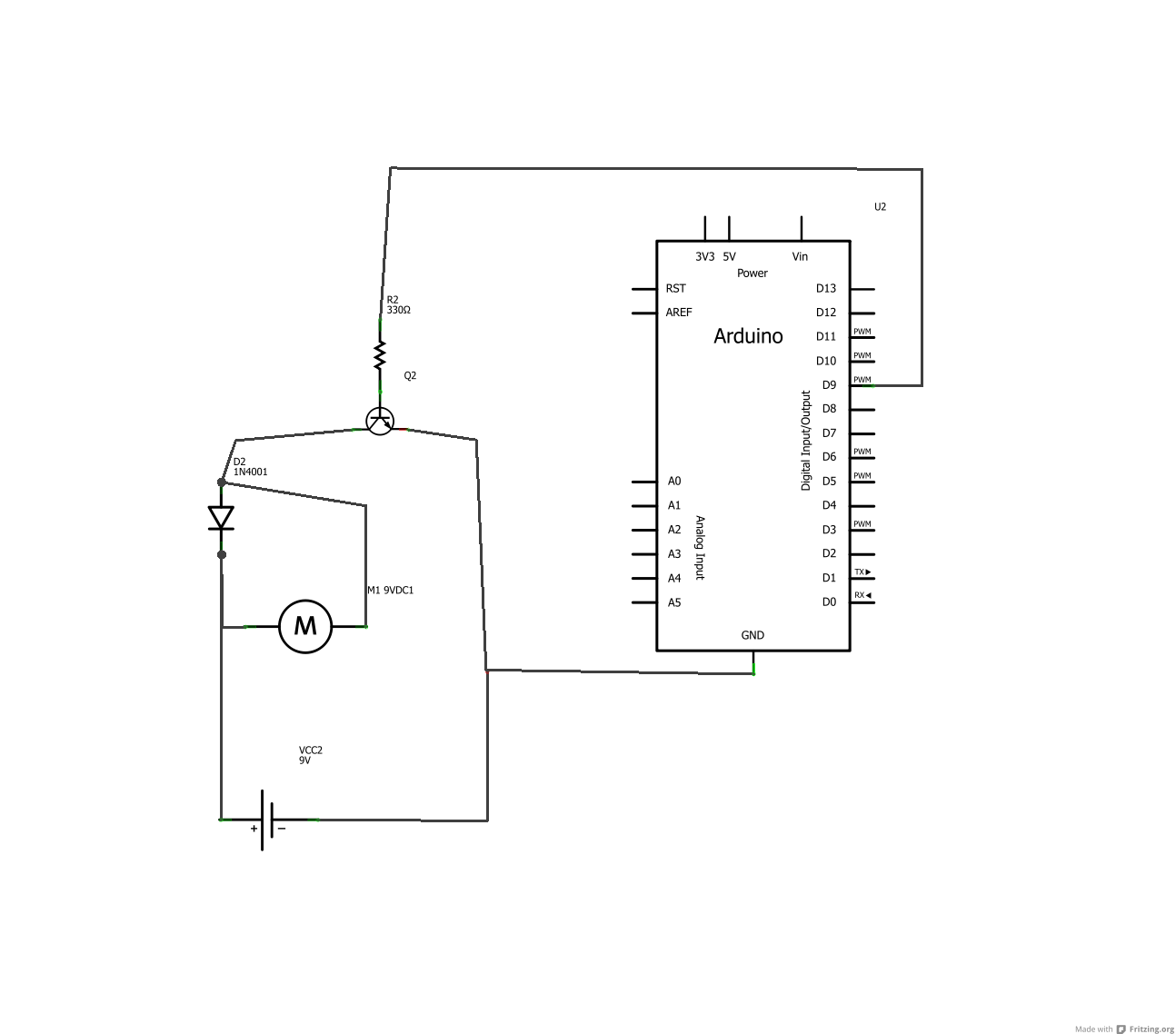
I've looked at a lot of project designs that use the TIP120, but wanted to verify the diagram that I came up with is correct and won't totally burn up my arduino.
I'm using USB to power the arduino, a 9v battery to power a cheap 9v DC hobby motor, a 2.2k Ohm resister between pin9 and the base on the TIP120. An IN4004 diode is wired in, as well as a small .1uF on the motor (to limit noise). There is a common ground with the arduino.
Am I correct that the TIP120 has a max of 60V 5A with a heatsink?
If I were to use an IRF510 MOSFET instead, would it be wired in the same, and just capable of 60V 16A max?
Your transistor needs to be mirrored - emitter to Gnd collector to the motor.
Current will from Batt+ to collector to emitter to Gnd when the base is supplied with current.
You may likely need a smaller base resistor also. You can experiment and safely go down to 150 ohm.
I changed the schematic - sorry, new to designing schematics too. So this design should cover controlling DC devices within the 5V-60V 5A range, depending on the device used in place of the motor and the battery used for powering the device, right?
Yes. For higher power, the transistor will need some decent heat sinking.
You would likely want to change to a low Rds/logic level/N-channel MOSFET which will run a lot cooler too.
A TIP120 is spec'ed at having Vce 4V @ 20mA, 5A, so its gonna be real hot.
A part like this
with 22 mOhm Rds will dissipate just 5A x 0.022ohm = 0.11W and need little to no heatsinking.
You could use the NPN to switch it low with a resistor pulling the collector high to overcome the input capacitance of the gate and ensure fast switching times from on to off, and off to on.
So the attached layout on a breadboard is how it should be wired up to match the schematic, correct?
I have an IRF510 N-channel MOSFET, which sounds like it would be a better option for higher power needs. Can I switch out the TIP120 for the IRF510, keeping same layout and same resistor? As I understand it, the TIP's Base, Collector, and Emiter are the MOSFET's Gate, Drain, & Source, respectively.
IRF510 would be okay if you had the NPN in front of it so the gate voltage can go higher than 5V. It really turns on full with Vgs = 10V, not 5V like the one I linked to.
IRF510 is designed for 10V gate drive, so not really suitable. In practice, it may be OK up to a couple of amps or so. Better to use a logic-level (i.e specified for 4.5V gate drive) mosfet instead.
Thanks for your help guys! Sorry for my confusion - I'm new to all this, and have looked at a few guides that have caused me some confusion. Some guides showed using the IRF510 in place of the TIP120, but it sounds like I'll want to use the SOT78 you linked to instead.
I've tried to understand the datasheets and electrical characteristics listed for the transistors, but bare with me - I'm still learning. So the Vgs, is the voltage applied to the gate to turn on/off higher current flow from source to drain, right?
So, just to make sure I'm understanding correctly, the SOT78 I can use in place of the TIP120, wired in exactly the same. And if I understand correctly, the SOT78 would allow me to control devices up to 30V max at 30A max, with a heatsink for those higher requirements.
You don't have the battery ground connected to the top rail for the Source to connect to. The Battery+ goes to the MOSFET Drain.
(confusingly named, I would agree).
See page 2 of the data sheet for the pin connections.
On the far right side of the image, I have the top and bottom rails linked, with the transistor source running to ground on the top rail, and the drain running to battery + through the diode. That should work, right?
Ah, smaller screen, didn't see that.
Yes, if the rails actually go the whole length. Some breadboards are split in half. Confirm yours with a meter. You are better off with shorter connections.

