Transistors - what is the collector/emitter voltage drop?

I've been trying to get my head around transistors again. I watched this video:

In that he said that whilst there was a 0.7V drop between base and emitter, because of the PN junction, there was "almost no" drop between collector and emitter because the PNP junction "cancelled it out". In fact he measured around a 0.1V drop between collector and emitter due to manufacturing issues.

Meanwhile, on this page (Transistors 101):

http://sunburst.usd.edu/~schieber/psyc770/transistors101.html

He says that:

2.) If the transistor is on, the Collector voltage is 1.6 volts higher than the Emitter voltage.

Both are using a similar circuit.

So they can't be both right, eh?
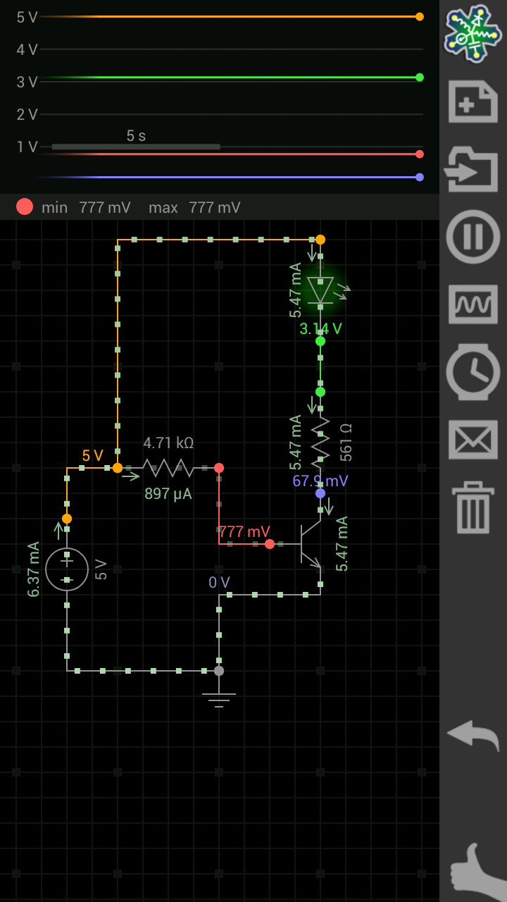
So I set up a test:

The LED had a forward voltage of 1.71 V.
The transistor had a Vbe of 0.872

The theoretical current through R1 would be:

(5 - 0.872) / 4700 = 0.000878  (0.878 mA)

Measured was 0.857 mA, so that is reasonably close.

The theoretical current through R2 would be:

(12 - 1.71) / 560 = 0.018375  (18.38 mA)

Measured was 18.57 mA, so that is pretty close.

I measured 12.06 V at the +12 V point, and 10.28 at point C, giving a voltage drop of 1.78 V in circuit.

I measured 60 mV at point D, so it would appear that the collector/emitter voltage drop was closer to 0.1V than 1.6V.

I measured 19.20 mA at point E, so that would be roughly the collector/emitter current plus the base/emitter current.

Does all that sound right? And does that make this quote incorrect?

If the transistor is on, the Collector voltage is 1.6 volts higher than the Emitter voltage.

Take a look a screenshot.

Thing is the voltage drop varies between transistors and the 2n2222 is guilty of a higher voltsge drop.

Both guys were using the 2N2222 transistor as far as I could tell.

Thanks for simulating that, basically your screenshot agrees with my measurements, yes?

I think that "Collector-Emitter Saturation Voltage" listed in the datasheet is the voltage drop across collector-emitter when the transistor is fully saturated. It is dependent on collector current. For example, the datasheet of 2N2222 reports VCE(sat) = 400mV for IC = 150 mA and IB = 15 mA and VCE(sat) = 1.6V when IC = 500 mA and IB = 50 mA.

EDIT: the values for 2N2222A are slightly better: 300mV and 1V. And these are "guaranteed max values", so probably the voltage drop is lower in practice.

For what it's worth, I have some 2N2222 transistors manufactured by Fairchild and some "generic". Both are well within specifications for 2N2222 transistors. However, the Fairchild transistors: 1. grossly exceed the specifications; 2. have a much tighter standard deviation.

Right. Well, do you agree, or not, that you might expect 1.4V or so voltage drop between collector and emitter (2 x 0.7V) or no voltage drop because they two voltage drops cancel out? (one positive, one negative)

You will never get no voltage drop, they do not cancel out that is a gross simplification.
You will always get some drop. This depends on the transistor, the temprature and the collector current, and the base current.
Data sheets give you the worst case, your measurements give you what you are seeing for your circumstances.

The voltage drop depends on whether or not the transistor is restricting the current Ice . If the current going into the base is high enough, and the collector current is restricted by another component (resistor / load) to well within the limits of the transistor, the voltage drop is going to be fairly small (0.1-0.2 V). In your sample circuit, restricting the base current by using a 47K resistor, and adding a few LED's (and resistors) in parallel with the existing one to decrease load resistance will probably result in a much higher voltage drop.

Pieter

Well, according to the PN2222 datasheet, if Ic is 10mA and Ib is 1mA, then the VCE(sat) is about 0.1V, so this is in line with your measurements.

See figure 4 in the following datasheet:
http://www.onsemi.com/pub_link/Collateral/PN2222-D.PDF

EDIT: corrected reference

doesn't make sense, does it ?

If I put two resistors in series, they don't cancel each other out.

1 Like

yep, I should have "bolded" the end of the sentence too, I don't understand it either :wink:

alnath:
.
.

doesn't make sense, does it ?

Yes it does. The lower the collector current the smaller the effect of the collector impedance and consequently a lower collector emitter voltage.

There are a couple of very good treatises on the subject here and here (scroll down to section "2.2.2 The h-parameters" in the second one).

Edited to add quote so that the post makes sense!

Disagree.

This best describes may experience with the upper-limit (0.1V under my test conditions as well)...
http://forum.arduino.cc//index.php?topic=194939.msg1439105#msg1439105
http://forum.arduino.cc//index.php?topic=194939.msg1439118#msg1439118

The "generic" transistors varied noticeably but were always less than 0.1V (within specifications). The voltage drop across the Fairchild transistors was lower and was essentially identical between transistors.

Unfortunately, the experiments were more than a year ago # and, because everything was within specifications, I did not keep my notes. So, you now know everything I know.

# A polite way of saying, "too long ago for me to remember the details."

In theory with a perfect transistor, Vce(sat) is zero, since the work-function for going from
metal to n-type to p-type to n-type back to metal is zero (by symmetry).

In practice you have both resistance within the transistor distributed across all parts,
and symmetry is broken because the emitter is heavily doped and the collector is
lightly doped.

Modern superbeta transistors approximate the theoretical ideal much closer than ancient
devices like the 2222 because the doping profile can be exquisitely controlled
with ion-implatation (diffusion is the old method), and Vsat figures as low as 10mV
are seen in datasheets for low currents.

In that he said that whilst there was a 0.7V drop between base and emitter, because of the PN junction, there was "almost no" drop between collector and emitter because the PNP junction "cancelled it out".

This observation is only true of a saturated transistor at low values of the collector current, and the explanation is just plain wrong. Transistor action is not intuitive and can't be explained with such simplistic concepts.

Vce(sat), Vce in the "saturation" mode of transistor action, can vary from about 0.1 V to > 10 V, depending on transistor type and collector current. Obviously, Vce in the unsaturated mode can be as large as the power supply voltage -- the transistor is off.

gm1mfn:

alnath:
.
.

doesn't make sense, does it ?

Yes it does. The lower the collector current the smaller the effect of the collector impedance and consequently a lower collector emitter voltage.

There are a couple of very good treatises on the subject here and here (scroll down to section "2.2.2 The h-parameters" in the second one).

Edited to add quote so that the post makes sense!

good links, I agree, but none of them make this

that you might expect 1.4V or so voltage drop between collector and emitter (2 x 0.7V)

make sense :wink:

that you might expect 1.4V or so voltage drop between collector and emitter (2 x 0.7V)

Well, that doesn't make sense because the CB junction is reverse biased, when considered as a simple PN junction, so the forward bias 0.7V of a simple PN junction does not apply to the CB junction, nor does it apply to the BE junction, either. A bipolar transistor is -much- more complex than just two diodes pointing in or out.

I suggest some deep reading on semiconductor physics if you really want to get a better understanding of this. All the graphs of transistor curves aren't going to do anything more than show you that it is what it is.

And no simple schematic symbol or simplified sketch of an NPN junction is going to help, either. You should have some understanding of the standard model (of physics). Some. Do you know what the N and P mean? What are "holes"?

Which part do you disagree with?

The saturation voltage is a peculiar spec which is not needed by MOSFETs. Bipolar junction transistors have worked for decades to get a Vsat down to 0.1 volt, but for a MOSFET it is 0.00000 volts.

The npn has a base p material swamped with electrons from collector to emitter, shorting out any diode drop artifacts. The geometries and impurities can get a low Vsat, but at a cost of voltage, gain, and every other trade off.