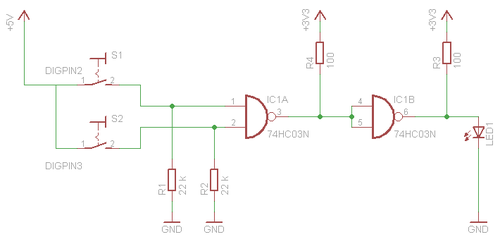
I've just started playing with Arduino, which is great, but my lack of experience/knowledge is starting to show. I recently picked up a few NAND ICs, namely 74HC03N from TI, and I'm attempting to make it work with the Arduino.
In this case, two NAND gates have been strung together to form an AND gate, which returns true if both inputs are positive. An LED is being used to display the output, and in this diagram the switches are being used to represent the digital pins on the Arduino.
It works, the LED lights when the two pins are HIGH, but what I am wondering is if this is the right way to do this with these gates, and secondarily, is it notated correctly in the diagram?
The gates are apparently 'open-drain' which I understand to mean it needs a pull-up resistor (that's what the data sheet is telling me anyway) to provide the output 'signal'.
Presumably the two 22k resistors (I inserted these while trying to work out why it wouldn't work, without these the LED just sits there and flickers if the pins are not HIGH) are there so that the gate inputs are always connected to GND not just 0v, but when the digital pins are HIGH the current can't be bothered to trudge through the resistor and most of it goes through the gate instead?
Apologies if these are stupid questions, or if this is not the right place to ask them, I'm off to the book store tomorrow to pick up a few books I think!
You can rely on INTERNAL pullups resistors or provide your own external pullup resistors on the outputs. It is sometimes easier to grasp the concept and usefulness of PULLUPS with logic gates by not relying on Internal Pullups in the Arduino.
The 1st logic gate would be ACTIVE = LOW outputs. IC1B inverts the logic levels. I Agree that the LED part of the circuit is not ideal.
Essentially, with OPEN DRAIN or OPEN COLLECTOR outputs, they get PULLED toward GND (or LOGIC LOW) potential and otherwise FLOAT (undetermined level) when not active.
To get a LOGIC 1 TTL level, you would rely in say an external 10K (100 Ohm = NOT GOOD) resistor between the logic gate output pin and 5V power source. This would then connect to ARDUINO input pin.
The ARDUINO would then see a "1" state passively through the resistor and then go to a LOW "0" state when the LOGIC GATE turns on and pulls the voltage level closer to GND potential. A high value resistor is needed to limit the current flow in the output of the gate so as not to "cook" it and let the magic smoke out.
That seems to make sense. With regards to LED resistor value, I used the formula
(VS - VL) / I
Where VS (3.3) is the supply voltage, VL (3.3) is the LED voltage and I (20mA) is the max current for the LED. (Light Emitting Diodes (LEDs))
With the LED I'm using it doesn't appear to need one (presuming I've done this right) when used with this supply, but I suppose it's a good idea to have one, just to protect it anyway? It reduces the brightness a bit as well so it's easier to have it sitting on the desk blinking away!
pwillard -
I'll have a think about you've said and try and get it working!
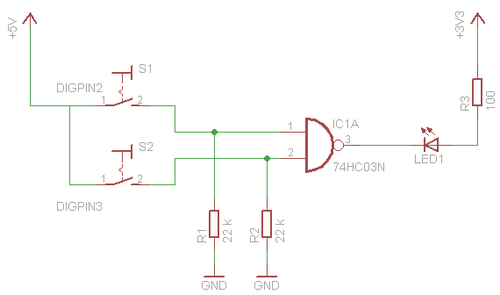
The inputs are all wrong for TTL. You don't pull down or at least if you do they need to be a bit smaller in value. The inputs are normally connected to the switches that are connected to ground. Then on the input is a pull up resistor of about 10K.
Yea, I think I realized to late that we are talking about outputs not inputs... but regardless... if you want TTL OUTPUT from an open drain/collector gate, you need a pullup.
Using ARDUINO DIGITAL PINS for OUTPUT into a NAND GATE, you would need neither PULLUP or PULL DOWN resistors. You would just directly drive the pins. It is the SWITCHES (having technically only 1 STATE) that need to rely on PULLUP or PULLDOWN.
In my case, I imagined (not yet seeing the missing drawing when I originally answered) that you wanted to feed the OUTPUT of the NAND to the arduino DIGITAL pin. In that case, you need to condition the voltage levels to match TTL using the method I described.
I now see that this is what you wanted... and it's that simple...
So, using NAND LOGIC... the LED ONLY lights up when PIN2 and PIN3 are both at logic "0". If any or both are LOGIC "1"... the LED is DARK.
The HC chips are made so that you need not be such picky with old fashioned "TTL", though it is a good thing to KNOW about it.
The 100 Ohms are fine. The OC/OD output had limitted your current to something around 25mA anyway, but it is safer to use that resistor..