I am working through the tutorial "Serial to Parallel Shifting-Out with a 74HC595". On page four of my printout there is a photo of the wiring and a circuit diagram. These do not agree.
//**************************************************************//
//  Name    : shiftOutCode, Hello World
//  Author  : Carlyn Maw,Tom Igoe, David A. Mellis
//  Date    : 25 Oct, 2006
//  Modified: 23 Mar 2010
//  Version : 2.0
//  Notes   : Code for using a 74HC595 Shift Register           //
//          : to count from 0 to 255
//  Modified: December 11, 2017
//  By      : Vagulus
//  Include : Debug Serial Output
//****************************************************************

#include <SPI.h>

//Pin connected to ST_CP of 74HC595
int latchPin = 8;
//Pin connected to SH_CP of 74HC595
int clockPin = 12;
//Pin connected to DS of 74HC595
int dataPin = 11;
//Debug output switch
const bool DEBUG = true;


void setup() {
	// set debug switch
	if (DEBUG) Serial.begin(9600);
	//set pins to output so you can control the shift register
	pinMode(latchPin, OUTPUT);
	pinMode(clockPin, OUTPUT);
	pinMode(dataPin, OUTPUT);
}

void loop() {
	// debug
	if (DEBUG) Serial.println("Starting the loop");

	// count from 0 to 255 and display the number
	// on the LEDs
	for (int numberToDisplay = 0; numberToDisplay < 256; numberToDisplay++) {
		// take the latchPin low so
		// the LEDs don't change while you're sending in bits:
		digitalWrite(latchPin, LOW);
		// shift out the bits:
		shiftOut(dataPin, clockPin, MSBFIRST, numberToDisplay);
		// tell the world number is printed
		if (DEBUG)
		{
			Serial.print("Displaying number ");
			Serial.println(numberToDisplay);
		}
		//take the latch pin high so the LEDs will light up:
		digitalWrite(latchPin, HIGH);
		// pause before next value:
		delay(500);
	}
}
and the serial output confirms the program is running. I have replaced both the UNO and the 74HC595 to no avail. I treble-checked both sets of wiring. Something is rotten in the state of Arduino .
Would someone please tell me how to get this running.
aarg:
Please specify the discrepancy instead of leaving us the job of finding it.
It transpires that the problem was the circuit diagram. The one attached works. This MOV shows it working - sorry about the quality. I don't know what went wrong there.
As is usual in electronics, everyone has their own nomenclature, one of the other two PNGs shows the terminology Texas Instruments use and I'm not going to argue with them. The last PNG shows the Serial Output of the debug code I inserted (see above).
Could someone with the necessary permissions change the tutorial accordingly. It seems futile to present a tutorial that is both inconsistent and incorrect. No-one can learn from something like that.
You're really living up to your name "vague-ulus". Why is it so hard for you to just say what's wrong? I'd happily submit a bug report to the Arduino developers if I can verify the error but I'm not going to waste time trying to reverse engineer what the necessary change is from some pictures when you could just write a few words and save me the trouble.
I think it's that 1uF cap on one of the 'data' lines in https://www.arduino.cc/en/Tutorial/ShiftOut; it has been pointed out numerous times to people that followed that link.
I just put both diagrams on my VDU and spotted the source of my confusion. The connections to the 74HV595 in the webpage are done by name and the pin positions by number are scrambled. This is the very sort of vague-ness that traps beginners like myself. (BTW pert, vagulus refers to a little traveler - the pilgrim in search of the truth ) In attempting to wire the circuit to that diagram I assumed that the outputs in the diagram were in the same physical place on the chip.
In the interests of clarity, I would like to see that diagram replaced with the one I sent which more closely represents the reality. Then dumbos like me wouldn't annoy august persons like yourselves. :-*
While we're about it, I found the code in Code Sample 1.2 One by One didn't teach me much. In battling to understand what was supposed to happen I re-wrote it.
/*
-- filename   : oneByOne.ino
--
-- purpose    : reads Serial Input, filters it, and uses the
--  result to set the pins of a 74HC595 shift register thus
--  lighting LEDs attached to the output pins of the shift register
--
-- derivation : Code Sample 1.2 in the Arduino "ShiftOut" tutorial
--               at https://www.arduino.cc/en/Tutorial/ShiftOut
--               written by Tom Igoe
--
-- version    : 0
--
-- date       : December 14, 2017
--
-- author     : Vagulus
--
1234567890123456789012345678901234567890123456789012345678901234567890
_________1         2         3         4         5         6         7
*/


//Pin connected to latch pin (ST_CP) of 74HC595
const int latchPin = 8;
//Pin connected to clock pin (SH_CP) of 74HC595
const int clockPin = 12;
////Pin connected to Data in (DS) of 74HC595
const int dataPin = 11;
// create working variable
int ledToLight = 0;
// debug switch
const bool DEBUG = true;


// forward declarations

// specify to the shift register which bit to set HIGH
//  then move it out to the 74HC595
void specifyHighBit(int ledToLight);
// clear Serial input buffer
void flushInputBuffer();


void setup()
{
	//set pins to output because they are addressed in the main loop
	pinMode(latchPin, OUTPUT);
	pinMode(dataPin, OUTPUT);
	pinMode(clockPin, OUTPUT);

	// start Serial
	Serial.begin(9600);

	// clear Serial input buffer
	flushInputBuffer();
}  // end setup()


void loop()
{
	// ASCII '0' through '7' characters are
	// represented by the values 48 through 55.
	// so if the user types a number from 0 through 7 in ASCII,
	// you can subtract 48 to get the actual value:


	  // invite data entry
	Serial.println("Enter a number 0..7");

	// wait for that entry
	while (Serial.available() == 0) {}

	// read in keyboard input as numeral value
	ledToLight = Serial.read() - 48;
	if (DEBUG)
	{
		Serial.print("Number entered was ");
		Serial.println(ledToLight);
	}

	// filter input to ensure data is in range
	if (ledToLight >= 0 && ledToLight <= 7)
		// write to the shift register with the correct bit set high:
		specifyHighBit(ledToLight);

	// clear Serial input buffer
	flushInputBuffer();
}  // end loop()

/*==========================================*/

// specify to the shift register which bit to set HIGH
//  then move it out to the 74HC595
void specifyHighBit(int ledToLight)
{
	// creating a variable with value  '0' gets a byte of eight '0's
	//  which would set all eight outputs of the 74HC595 to LOW
	byte eightZeros = 0;

	// turn off the output so the pins don't light up
	// while you're shifting bits
	digitalWrite(latchPin, LOW);

	//NOTE:
	// here you are writing to the variable (eightZeros)
	//  in which each bit is LOW (zero)
	// this instruction turns on the specified bit:
	bitWrite(eightZeros, ledToLight, HIGH);

	// smove the variable into the memory of the shift register
	shiftOut(dataPin, clockPin, MSBFIRST, eightZeros);

	// turn on the output so the LEDs can light up:
	digitalWrite(latchPin, HIGH);
}  //  end specifyHighBit()

/*==========================================*/

// clear Serial input buffer
void flushInputBuffer()
{
	// local variable
	byte byteDump;

	// give Serial Input time to catch up
	delay(10);

	// read the buffer until it is empty
	while (Serial.available() > 0)
	{
		byteDump = Serial.read();
		if (DEBUG)
		{
			Serial.print("Character read was ");
			Serial.println(byteDump);
		}
	}
}  // end flushInputBuffer()
I think that this step-by-step process is easier for the beginner to follow, and the sketch does solve the problem created by the IDE I use (Visual Studio/Visual Micro) which inserts a NL character after the digit entered. It does this using the function flushInputBuffer().
Before someone gets upset about me using VS/VM, my geriatric eyesight makes reading the Arduino IDE very difficult on a 4K VDU. VS/VM is much more legible.
Your request is still murky to the casual reader. Why not make it easy and post the offending image in-line, along with a clear explanation of the problem and proposed solution? Like so:
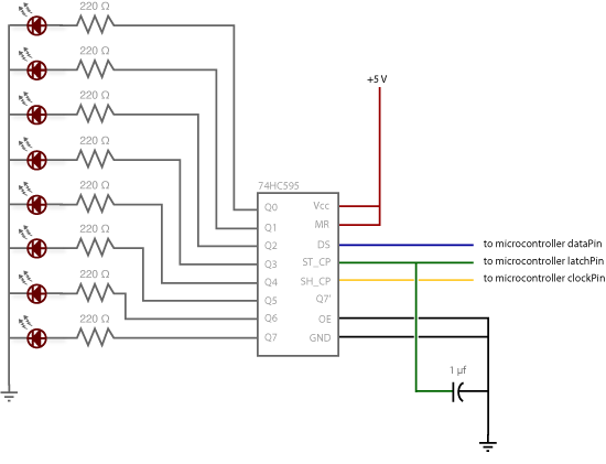
His objection is that the pin arrangement in this image from the tutorial (call it image "A")...
...does not match the chip pin-out from the tutorial ("B")...
...so, someone (like the OP, apparently) who blindly connects wires assuming the chip pin locations are as shown in "A" (ignoring the tutorial's step-by-step images shown below, and not double-checking the wiring against the datasheet pin-out, as in "B"...it's always a good idea to check the datasheet pin-out) will obviously be making many mistakes (and, perhaps, permanently damaging their chip).
Tutorial step 1
Tutorial step 2
Tutorial step 3
So, the OP seems to be proposing to replace "A" with the following image ("C") or, presumably, one similar to "C," but "prettied up" to match the tutorial style and some normal schematic conventions (like not having the UNO upside down, for starters).
vagulus:
In the interests of clarity, I would like to see that diagram replaced with the one I sent which more closely represents the reality. Then dumbos like me wouldn't annoy august persons like yourselves.
Schematics are laid out so as to clarify the function of the circuit, so they normally follow a logical layout, not a physical one. You should get used to it as that is how the vast majority are drawn.
Drawing schematics in a rats nest style, according to the physical layout of a chip, is very uncommon, and for good reason, such schematics are difficult to read.
the interests of clarity, I would like to see that diagram replaced with the one I sent which more closely represents the reality.
No no no.
The point of a schematic is to show the interconnections in as clear a way as possible. This means the minimum of wires crossing. This can only be achieved most of the time by not matching the physical layout. Get Fritzing out of your head, you do not need to have a physical representation in schematics unless it is helpful like where layout is important or you are using a none standard or custom component.
Schematic rules are
Positive at the top negitave at the bottom
Minimum wire crossing
Signal flow where possible from left to right
Only horizontal and vertical wires
Minimum use of common connection symbols, powe and ground are fine but think twice about anything else.
Use bus wiring to minimises repetive and spagetty like wiring.
Label all connections into in IC with pin number and where appropriate pin name
We can’t even get wrong stuff removed, what makes you think we can correct stuff that is right with wrong stuff?
DaveEvans:
...so, someone (like the OP, apparently) who blindly connects wires assuming the chip pin locations are as shown in "A"
I suspect that's exactly what many beginners, like myself, do! It's like connecting the dots when you are learning to draw. Some time is likely to elapse before I am sufficiently knowledgeable to wire up a chip working on the function of each connection.