Help with Mux and Demux using Arduino Due

Hello i have been working on this for a few months now, trying to make a multi master/slave 4051 mux/demux. It as taken me that long as i am still very new with arduino, and this was my first real project.

So what this does is:
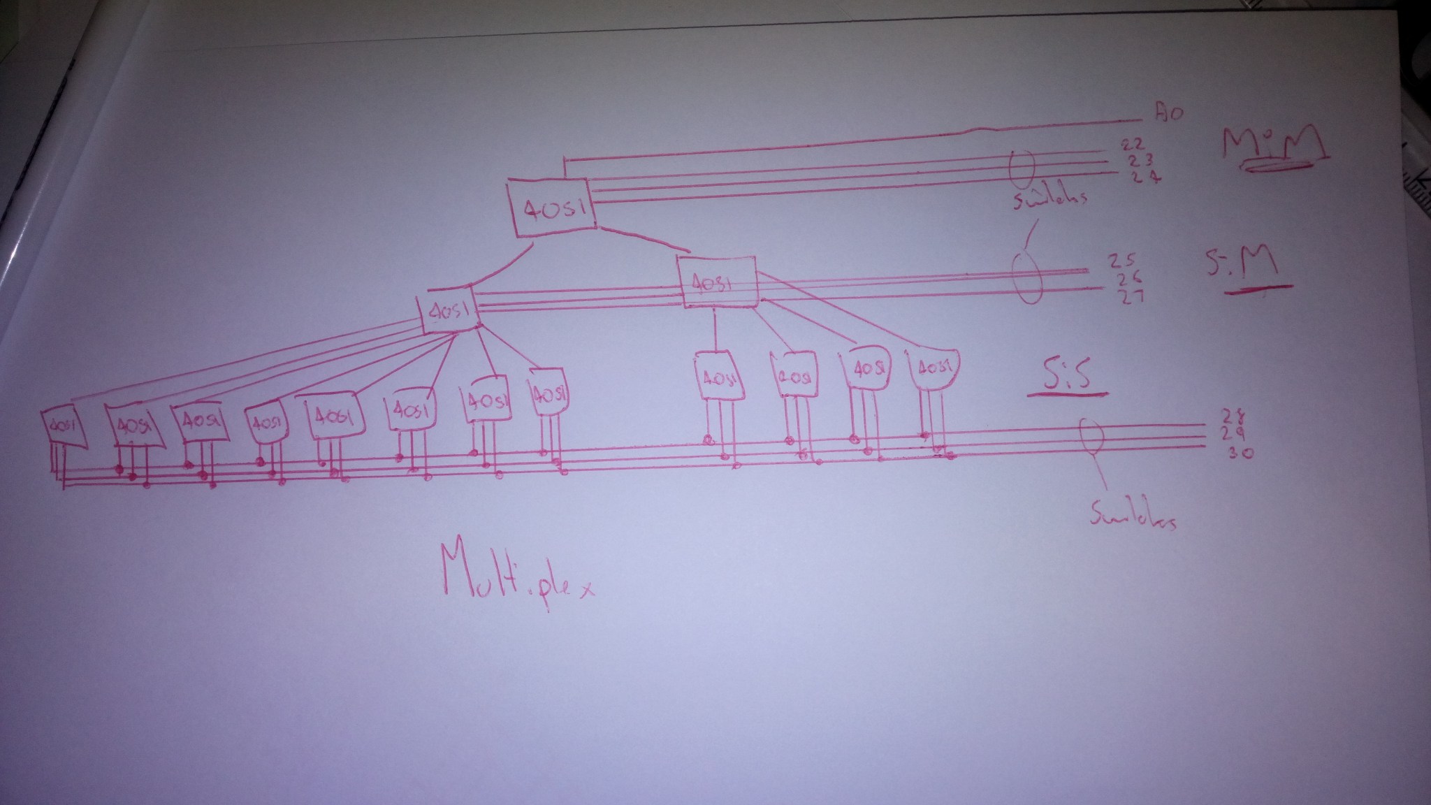
Arduino Due receives analog voltage from a potentiometer (A0) through mux's then sends it out to demux's (DAC0)

Mux = Potentiometer --> "SiS" --> "SiM" --> "MiM" --> "Arduino Due"
DeMux = "Arduino Due" --> "MoM" --> "SoS"

my problem is it takes to long to do a complete loop from SiS, SiM and MiM = 0 to SiS and SiM = 7 and MiM = 2 and through to MoM and SoS = 0 to MoM = 2 and SoS = 7 and because of this the voltage drops from 2.7v to 0.16v
so i was thinking if i could shorten this code some how like using port manipulation but i couldn't really find much information on that. it maybe that there's to much code to go through to be able to complete it in < 1ms

thank you :slight_smile:

int SiS = 0;  int SiM = 0;  int MiM = 0;

void setup(){
  for(int i = 22; i < 37; i++){pinMode(i, OUTPUT);}  
}

void loop(){

//cycler    
SiS++;
if (SiS > 7) { SiM++; SiS = 0; 
if (SiM > 7) { MiM++; SiM = 0;} }
if (MiM > 2) {MiM = 0;} 

//SiS setup
if (SiS == 0){ digitalWrite(24, LOW); digitalWrite(23, LOW); digitalWrite(22, LOW);     digitalWrite(33, LOW); digitalWrite(32, LOW); digitalWrite(31, LOW);}     //0
if (SiS == 1){ digitalWrite(24, HIGH); digitalWrite(23, LOW); digitalWrite(22, LOW);    digitalWrite(33, LOW); digitalWrite(32, LOW); digitalWrite(31, HIGH);}    //1
if (SiS == 2){ digitalWrite(24, LOW); digitalWrite(23, HIGH); digitalWrite(22, LOW);    digitalWrite(33, LOW); digitalWrite(32, HIGH); digitalWrite(31, LOW);}    //2
if (SiS == 3){ digitalWrite(24, HIGH); digitalWrite(23, HIGH); digitalWrite(22, LOW);   digitalWrite(33, LOW); digitalWrite(32, HIGH); digitalWrite(31, HIGH);}   //3
if (SiS == 4){ digitalWrite(24, LOW); digitalWrite(23, LOW); digitalWrite(22, HIGH);    digitalWrite(33, HIGH); digitalWrite(32, LOW); digitalWrite(31, LOW);}    //4
if (SiS == 5){ digitalWrite(24, HIGH); digitalWrite(23, LOW); digitalWrite(22, HIGH);   digitalWrite(33, HIGH); digitalWrite(32, LOW); digitalWrite(31, HIGH);}   //5
if (SiS == 6){ digitalWrite(24, LOW); digitalWrite(23, HIGH); digitalWrite(22, HIGH);   digitalWrite(33, HIGH); digitalWrite(32, HIGH); digitalWrite(31, LOW);}   //6
if (SiS == 7){ digitalWrite(24, HIGH); digitalWrite(23, HIGH); digitalWrite(22, HIGH);  digitalWrite(33, HIGH); digitalWrite(32, HIGH); digitalWrite(31, HIGH);}  //7
//SiM setup
if (SiM == 0){ digitalWrite(27, LOW); digitalWrite(26, LOW); digitalWrite(25, LOW);;}    //0
if (SiM == 1){ digitalWrite(27, HIGH); digitalWrite(26, LOW); digitalWrite(25, LOW);}    //1
if (SiM == 2){ digitalWrite(27, LOW); digitalWrite(26, HIGH); digitalWrite(25, LOW);}    //2
if (SiM == 3){ digitalWrite(27, HIGH); digitalWrite(26, HIGH); digitalWrite(25, LOW);}   //3
if (SiM == 4){ digitalWrite(27, LOW); digitalWrite(26, LOW); digitalWrite(25, HIGH);}    //4
if (SiM == 5){ digitalWrite(27, HIGH); digitalWrite(26, LOW); digitalWrite(25, HIGH);}   //5
if (SiM == 6){ digitalWrite(27, LOW); digitalWrite(26, HIGH); digitalWrite(25, HIGH);}   //6
if (SiM == 7){ digitalWrite(27, HIGH); digitalWrite(26, HIGH); digitalWrite(25, HIGH);}  //7
//MiM setup
if (MiM == 0){ digitalWrite(30, LOW); digitalWrite(29, LOW); digitalWrite(28, LOW);     digitalWrite(36, LOW); digitalWrite(35, LOW); digitalWrite(34, LOW); }     //0
if (MiM == 1){ digitalWrite(30, HIGH); digitalWrite(29, LOW); digitalWrite(28, LOW);    digitalWrite(36, LOW); digitalWrite(35, LOW); digitalWrite(34, HIGH); }    //1
if (MiM == 2){ digitalWrite(30, LOW); digitalWrite(29, HIGH); digitalWrite(28, LOW);    digitalWrite(36, LOW); digitalWrite(35, HIGH); digitalWrite(34, LOW);}     //2
  
analogWrite(DAC1, analogRead(A0)); 
}

I must be new too because I don't understand your acronyms. "Man in the middle"? "Something is smelly?"

The variable names are "free" in Arduino. You don't save any space by using short names. You just make it harder for yourself (and anyone else) to read. Here's an example of a program I wrote a long time ago:

  if(User_Is_An_Idiot_and_Cant_Spell) {
    helpUserSpelling();
  }

Now, isn't it obvious to you - without any other context - what this program is doing in this tiny snippet?

Don't put all the statements on one line. The braces allow you to split an if() statement across many lines, for readability. Use the auto-formatter on the Arduino Tools menu.

And finally, don't use "magic numbers" in your program. What is 28, what is 30? Give those pin numbers meaningful names at the top of the program. Then if you ever change pins - which happens more often than you think - it's easy to change in one place instead of doing a search-replace on "30" which might screw up some other part of the code which used the number "300".

trying to make a multi master/slave 4051 mux/demux.

OK what is one of these?
Can you please post a schematic?
Can you say what you want it to do?

Did you know that you don't get the full range of voltage on a Due's D/A pin.

MorganS:
I must be new too because I don't understand your acronyms. "Man in the middle"? "Something is smelly?"

The variable names are "free" in Arduino. You don't save any space by using short names. You just make it harder for yourself (and anyone else) to read. Here's an example of a program I wrote a long time ago:

  if(User_Is_An_Idiot_and_Cant_Spell) {

helpUserSpelling();
 }


Now, isn't it obvious to you - without any other context - what this program is doing in this tiny snippet?

Well "SiS", "SiM" and "MiM" used to be "SS", "SM" and "MM" respectively being an acronym for "Slave Slave", "Slave Master" and "Master Master" but i kept on getting errors, and it turned out that SS was used for Serial or something like that. So I just added the lower case I in the middle so I would know that it's an input if I needed it for something else
But yea I probably should of changed from the acronyms to the full thing so it would be easier to read.

MorganS:
Don't put all the statements on one line. The braces allow you to split an if() statement across many lines, for readability. Use the auto-formatter on the Arduino Tools menu.

Yea I know you can but the statements on multi lines I just thought it would be easier to see the difference between each if statement by just having it on the single line, but it does look harder to read now you said that

MorganS:
And finally, don't use "magic numbers" in your program. What is 28, what is 30? Give those pin numbers meaningful names at the top of the program. Then if you ever change pins - which happens more often than you think - it's easy to change in one place instead of doing a search-replace on "30" which might screw up some other part of the code which used the number "300".

That is very true i don't know why I didn't do that. I will change it now
Thank you very much for the feedback and help

Grumpy_Mike:
OK what is one of these?

Gif rerpreesnting what it does

Truth table

this is a very good photo explaining what a multiplex does
but pretty much its just an electronic rotary switch which changes it position depending on the state of the 3 switch inputs

Grumpy_Mike:
Can you please post a schematic?

What schematic creator would you recommend me using as my schematic is on paper.

Grumpy_Mike:
Can you say what you want it to do?

I would like it so that the arduino will have more analog inputs and more analog outputs

Grumpy_Mike:
Did you know that you don't get the full range of voltage on a Due's D/A pin.

Yes its something like 0.5 - 2.7v, isnt it?

What schematic creator would you recommend me using as my schematic is on paper.

Photograph the paper and post the picture.

I would like it so that the arduino will have more analog inputs and more analog outputs

I didn't see any analogue outputs in that gif only inputs. While the 4051 is great for multiplexing inputs it is useless for multiplexing outputs because the voltage output only appears while that channel is being addressed. What you need is something with an analogue output latch like a sample and hold circuit, but those suffer from leakage if you hold the output for too long.

Your code seems to be using 6 multiplex address select pins. This implies that you have 64 analogue inputs or some very poor design. That is why we ask for a schematic.
If you learned to use arrays then your code would not have to be so turgid. This page might help you cut it down considerably.
http://www.thebox.myzen.co.uk/Tutorial/Arrays.html

@xSuChisLiF3x :

If I understand what you are willing to do, you want to experiment your DUE's ADC and DAC controllers througt out a project using 4051 mux/demux ?

If this is the case, I suggest you to begin with a more simple project using ADC ---> DAC controllers for example between AO and DC0.

As you may know, the ADC controller input should be in the range of : 0V <--> 3.3V and the DAC controller outputs a voltage between : 1/6 * 3.3V <---> 5/6 * 3.3V .

Once you have managed to code your ADC and DAC controllers, then you can upgrade your project with the 4051 mux/demux. :slight_smile:

You may also know that the DAC controllers need to be used with a load of several K Homs, 10 K Homs would be safe for starting. Without these loads, you will probably burn your DACs ! :confused: :confused:

Btw : there is a relevant information on the right way to use 4051 mux/demux here : Arduino Playground - 4051

You may also know that the DAC controllers need to be used with a load of several K Homs, 10 K Homs would be safe for starting. Without these loads, you will probably burn your DACs ! :confused: :confused:

Sorry that is totally wrong. Without any load the D/A output is fine. It is only when a load is such that you get a current of 3mA or greater that you can burn out the A/D pin and this is only A/D 0, the A/D 1 pin has greater current capability.
So a load of 1K5 ohms is the maximum you should use.

Grumpy_Mike:
Photograph the paper and post the picture.

See atachments

Grumpy_Mike:
I didn't see any analogue outputs in that gif only inputs.

The "faders" on the right side are the analog inputs which depending on the switch states the "analog in signal" is the input from "faders"

Grumpy_Mike:
While the 4051 is great for multiplexing inputs it is useless for multiplexing outputs because the voltage output only appears while that channel is being addressed. What you need is something with an analogue output latch like a sample and hold circuit, but those suffer from leakage if you hold the output for too long.

http://www.onsemi.com/pub_link/Collateral/MC74HC4351-D.PDF you mean something like this?

Grumpy_Mike:
Your code seems to be using 6 multiplex address select pins. This implies that you have 64 analogue inputs or some very poor design. That is why we ask for a schematic.

I have in total 15 4051's and 96 analog inputs for multiplexing and 4 4051's and 24 analog outputs for the Demultiplexer but you can see this in the schematic. I know its not a real schematic but i was trying for ages to have all the wires but it got to messy and unreadable.

Grumpy_Mike:
If you learned to use arrays then your code would not have to be so turgid. This page might help you cut it down considerably.
http://www.thebox.myzen.co.uk/Tutorial/Arrays.html

This looks very interesting and helpful i will look into this thank you

ard_newbie:
@xSuChisLiF3x :

If I understand what you are willing to do, you want to experiment your DUE's ADC and DAC controllers throughout a project using 4051 mux/demux ?

If this is the case, I suggest you to begin with a more simple project using ADC ---> DAC controllers for example between AO and DC0.

Yea i did try this after realising that the output voltage from the demux was so low. I set up 1 mux and 1 demux reading and writing from A0 and DAC0 respectively and it gave me my desired result

ard_newbie:
Btw : there is a relevant information on the right way to use 4051 mux/demux here : Arduino Playground - HomePage

To be honest i could not make sense of that example, i know it had some things to to do with bits
"r0 = bitRead(count,0);"but after reading through the references of that i still could make out what the tutorial was saying. i understand the count for loop but not the bitread.

Grumpy_Mike:
Sorry that is totally wrong. Without any load the D/A output is fine. It is only when a load is such that you get a current of 3mA or greater that you can burn out the A/D pin and this is only A/D 0, the A/D 1 pin has greater current capability.
So a load of 1K5 ohms is the maximum you should use.

so i should use DAC1 instead just to be on the safe side?
But i dont think it draws that much d=current so i dont need to worry about it?

@xSuChisLiF3x

To be honest i could not make sense of that example, i know it had some things to to do with bits
"r0 = bitRead(count,0);"but after reading through the references of that i still could make out what the tutorial was saying. i understand the count for loop but not the bitread.

Well, the tutorial explains how you can multiplex your inputs via S0, S1, S2.

In binary, if you consider that S0 is bit 0, S1 is bit 1 and S2 bit 2, then:

when count = 0b000, it will signify that you choose Y0 as THE input,
when count = 0b001 " "Y1 " ",

and so on

when count = 0b111 " " Y7 " "

The count in the loop is masked with an " & " logic to extract the 3 bits you need to drive your multiplexer.

So you need 3 digital outputs to drive your multiplexer wired to S0, S1 and S2 pins. These digital outputs will be controlled by the above bit manipulation at the frequency of a complete cycle in the loop. This is why count vary between 0 and 7 to select respectively Y0 then Y1 then ..etc..Y7 as an input.

You can choose either DAC0 or DAC1 as long as you protect them with résistors in serial. And the only output Z will be wired directly to A0 ONLY IF the voltage range is between 0V and 3.3 V. If it's not the case, use some other device to come back in the right range.

ard_newbie:
@xSuChisLiF3x

To be honest i could not make sense of that example, i know it had some things to to do with bits

"r0 = bitRead(count,0);"but after reading through the references of that i still could make out what the tutorial was saying. i understand the count for loop but not the bitread.


Well, the tutorial explains how you can multiplex your inputs via S0, S1, S2.

In binary, if you consider that S0 is bit 0, S1 is bit 1 and S2 bit 2, then:

when count = 0b000, it will signify that you choose Y0 as THE input,
when count = 0b001 " "Y1 " ",

and so on 

when count = 0b111 " " Y7 " "

The count in the loop is masked with an " & " logic to extract the 3 bits you need to drive your multiplexer.

So you need 3 digital outputs to drive your multiplexer wired to S0, S1 and S2 pins. These digital outputs will be controlled by the above bit manipulation at the frequency of a complete cycle in the loop. This is why count vary between 0 and 7 to select respectively Y0 then Y1 then ..etc..Y7 as an input.


You can choose either DAC0 or DAC1 as long as you protect them with résistors in serial. And the only output Z will be wired directly to A0 ONLY IF the voltage range is between 0V and 3.3 V. If it's not the case, use some other device to come back in the right range.

Thank you so much that makes sence now. I knew the switches were 3 bit but just disnt make sense o the bitread but now i do.
So i would make three different for loops for each trio of wires for the pin selector of the 4051?
If so i will start working on it tomorrow, thamks

Thanks for the block diagram, although I would call them both multiplexers.
However they don't show much do they. Things like power supply, ground, enable inputs and decoupling spring to mind as missing.

i was trying for ages to have all the wires but it got to messy and unreadable.

What you need to do when you have a lot of wires all going to the same chips it to use the 'bus' wiring convention. Like this:-

seven seg bus.png

http://www.onsemi.com/pub_link/Collateral/MC74HC4351-D.PDF you mean something like this?

No, that has a latch on the address lines not the analogue output. I have never come across a chip with a latch on an analogue output so all I could think of is a sample and hold circuit on each output. As I said I think the analogue output multiplexer is a non starter.

You can use bit read but that is a bit babyish, my arrays page shows you the best way to do it with masking AND operations.

ard_newbie:
You can choose either DAC0 or DAC1 as long as you protect them with résistors in serial.

Sorry wrong again. You do not need any series resistors, in fact including them is detrimental to making the circuit work correctly. We have quality standards here and you are falling below them.

so i should use DAC1 instead just to be on the safe side?

Yes that would be safer.

Grumpy_Mike:
Thanks for the block diagram, although I would call them both multiplexers.
However they don't show much do they. Things like power supply, ground, enable inputs and decoupling spring to mind as missing.
What you need to do when you have a lot of wires all going to the same chips it to use the 'bus' wiring convention. Like this:-

seven seg bus.png

I didnt include VCC, GND, VEE and Enable in the drawing as:
VCC would come from 5v on arduino and go to all of the 4051's
GND, Enable and VEE are all joined together and go to ground
What is decoupling spring?

Bus wiring seems very smart and time efficient, i will use this on the schematic that i make using a computer schematic tool so i can easily edit the schematic. What Schematic tool would you recommend? Schemeit, Eagle?

Grumpy_Mike:
No, that has a latch on the address lines not the analogue output. I have never come across a chip with a latch on an analogue output so all I could think of is a sample and hold circuit on each output.

So wouldn't a sample and hold circuit make the analog signal a somewhat square wave?
for example this: http://www.brown.edu/Departments/Engineering/Courses/En123/graphicsSA/sach0.gif

Grumpy_Mike:
As I said I think the analogue output multiplexer is a non starter.

you mean this? "While the 4051 is great for multiplexing inputs it is useless for multiplexing outputs because the voltage output only appears while that channel is being addressed. What you need is something with an analogue output latch like a sample and hold circuit, but those suffer from leakage if you hold the output for too long."
if so what would you recommend as an alternative, if there is one?

Grumpy_Mike:
You can use bit read but that is a bit babyish, my arrays page shows you the best way to do it with masking AND operations.

So ive read your page like 6 times now from top to bottom and reread the references for bitwise operations. Should i have the one bit mask for all 3 SiS, SiM and MiM trio of switches or one for each trio

Sorry for all the question but i appreciate the help so much :slight_smile:

What is decoupling spring?

Har har :slight_smile: :slight_smile:
It is a missing comma, read that as:-
Things like power supply, ground, enable inputs and decoupling, spring to mind as missing.

So wouldn't a sample and hold circuit make the analog signal a somewhat square wave?
for example this: http://www.brown.edu/Departments/Engineering/Courses/En123/graphicsSA/sach0.gif

No it does not make is square, why would it? The switch charges up the capacitor to the voltage on the input to the switch and then the op-amp working as a voltage follower holds that voltage. It is a pure analogue circuit. What you have to ensure is that the switch, if it is electronic does not discharge the capacitor when it is supposed to be open.

Should i have the one bit mask for all 3 SiS, SiM and MiM trio of switches or one for each trio

Not sure I understand the question. The point is that you can use just one variable to increment and the value in it is the bits you need to transfer to the address lines of the multiplexer. You could do this as one variable for the first level of multiplexing and another variable for the second. Or you could just use one variable with the most significant bits controlling the first level multiplexer and constrain the value of the variable by resetting it back to zero when it reaches a certain value.

if so what would you recommend as an alternative, if there is one?

Apart from a sample and hold the only real option is an external multi channel A/D chip ( or two )

Grumpy_Mike:
No it does not make is square, why would it? The switch charges up the capacitor to the voltage on the input to the switch and then the op-amp working as a voltage follower holds that voltage. It is a pure analogue circuit. What you have to ensure is that the switch, if it is electronic does not discharge the capacitor when it is supposed to be open.

Dunno :frowning:
After reading about these "sample and hold analog latch" i will need one for each of the outputs of the output mux and instead of using a physical switch i would need top use an electric switch maybe a optocoupler? which is controlled by a pin on the due. but if i have 24 outputs from the mux i should use a shift register to control the optocouplers so i use up less pins? the "595" has a 100Mhz frequency cycle which if im not mistaken is the same as a clock cycle? if so it is more than enough for my use, as the due only has an 84Mhz clock cycle?
https://www.nxp.com/documents/data_sheet/74HC_HCT595.pdf

Grumpy_Mike:
Not sure I understand the question. The point is that you can use just one variable to increment and the value in it is the bits you need to transfer to the address lines of the multiplexer. You could do this as one variable for the first level of multiplexing and another variable for the second. Or you could just use one variable with the most significant bits controlling the first level multiplexer and constrain the value of the variable by resetting it back to zero when it reaches a certain value.

Sorry about that i meant multiple levels of mux's, as you just stated.
I will start playing around with bit masks, im thinking of using led's for each of the mux switch lines so i can test out how my bit mask goes.

Grumpy_Mike:
Apart from a sample and hold the only real option is an external multi channel A/D chip ( or two )

Do you mean that for a replacement for the mux input, otherwise that seems pointless for the dac as it defeats the purpose of it.

thanks again :slight_smile:

After reading about these "sample and hold analog latch" i will need one for each of the outputs of the output mux

Correct.

instead of using a physical switch i would need top use an electric switch maybe a optocoupler?

The switch you use is the output of the multiplexer. But as I said that might have an effect discharging the capacitor when it is not addressed so you either have to refresh it more often or use a voltage follower on the input to the capacitor as well as the output. You do not need any shift registers.

that seems pointless for the dac as it defeats the purpose of it.

You will see lots of analogue input multiplexers but you will not see many, if any, output analogue multiplexers. This is because it is difficult to do and using a sample and hold, which is the only real way to do it, compromises the voltage output integrity, especially for higher resolution outputs. If this is just an exercise then fine use a sample and hold, but if this has a real application with real constraints on the signal output integrity the only answer is multiple D/A's despite whether you think it defeats the purpose or not.

Grumpy_Mike:
You will see lots of analogue input multiplexers but you will not see many, if any, output analogue multiplexers. This is because it is difficult to do and using a sample and hold, which is the only real way to do it, compromises the voltage output integrity, especially for higher resolution outputs. If this is just an exercise then fine use a sample and hold, but if this has a real application with real constraints on the signal output integrity the only answer is multiple D/A's despite whether you think it defeats the purpose or not.

My analog output doesn't have to be that high of a resolution,maybe 8-bit.
Yes this will have a real purpose.
After looking around on google for ages as you said there's not many DAC's all i can really find is a "MCP4725" which is a single channel i2c breakout board, which means i will have to get 24 of them, that's a lot of $$$.
So i will make a "sample and hold analog latch" tomorrow and see how it goes

all i can really find is a "MCP4725" which is a single channel i2c breakout board

The ADR7317r has four D/A channels in one chip, as does the TLV5620.

Then these is this which is 8 channels.
http://uk.rs-online.com/web/p/products/7589610/?grossPrice=Y&cm_mmc=UK-PLA-_-google-_-PLA_UK_EN_Semiconductors-_-Data_Converters&mkwid=s0lyZ5oHJ_dc|pcrid|88057061523|pkw||pmt||prd|7589610&gclid=Cj0KEQjwl-e4BRCwqeWkv8TWqOoBEiQAMocbP4j2UZliGD3pzPBt8DklBLPPVE2l9iwngnqO3jN46R0aArvy8P8HAQ