Goal: Possibility to programmatically switch 3.3V peripherals (sensors, RF module) on an 3.3V Arduino on and off.
Question: What are the correct values for R1 and R2?


I've tried to figure out the values for R1 and R2 for a while now but couldn't find an example nor an understandable explanation on how to calculate their values. I'd really appreciate if someone could point me to a possible solution.
Thanks!
[Edit]

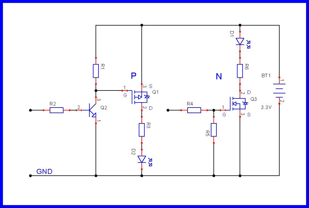
This is revision 1 of the schematic that I've modified according to the inputs given so far:
- In the original schematics the emitter of the transistor was connected to VCC instead of GND.
- This revision uses an NDP6020P logic level MOSFET instead of an FQP47P06.
- There is now a 10kΩ pull-down resistor at the Arduino pin D4.
- R1 is now 260kΩ and R2 33kΩ, which must be verified.
The circuit is part of a battery powered IOT application where a minimal power consumption and voltage drop are crucial. After some research I came to the above solution to switch all unused components off while an Atmega328P is in deep sleep.
The LED is just an example of a consumer, in reality this would be at least an HC-12 433 MHz HF module and one or more sensors which together will probably use 1 A max.
[End Edit]
FQP47P06-1009447.pdf (779 KB)
PN2222-D.pdf (122 KB)