PWM triggered ADC with Event line

Hi guys,

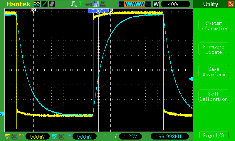
I'm trying to achieve an ADC sampling triggered by then PWM. The circuit is very simple, I have an RC filter on the PWM (pin 34 and 35, PWM ch0), and i'm reading the voltage on the capacitor trough the ADC, on pin A7 (ADC ch0).

As you can see in the image I would like to read the value at half of the transitory, because it's the average voltage.

Reading in the Arduino due ARM chip datasheet at page 1318 you can see that the Arduino due is equipped with a PWM event line, created for this purpose.

I'm pretty good with the registers so I used this way to implement the code. The problem is that the trigger is not reaching the ADC converter, and i don't know why, it's two weeks that I'm trying to figure out why. Meanwhile i wrote a code that uses another PWM (ch4, pin 9),synchronized with the ch0, that is doing the same job wired to the hardware trigger on pin 18. But I need a better solution, an external wire it's not enough for my project. In this case it's working, but I need something better. I also tried to ask to the Atmel support, but the path to reach their engineers is long and nobody gave me the right hint.

On the page 995 of the datasheet you can find how the event line works, it shouldn't be hard to do but for some reason I'm not able to deliver it.

Here my code, the register ADC_MR it's available in three modes, FREERUN (Never wait for a trigger, it's working), External trigger (it's working if you wire the Pin 18 to PWM on pin 9) and event line, that it's not working.

I hope someone of you can help me to deliver this event line trigger.

Have a good day.

unsigned int start_time;
unsigned int stop_time;
unsigned long values[1000];
void setup() {
  Serial.begin(250000);
  //PWM configuration
  REG_PIOC_PDR = PIO_PDR_P2 | PIO_PDR_P3 | PIO_PDR_P21; //PIO disable register of PC2, PC3 and PC23(pin34, pin35, pin9)
  REG_PIOC_ABSR = REG_PIOC_ABSR | PIO_ABSR_P2 | PIO_ABSR_P3 | PIO_ABSR_P21; //periphal AB select register for PC2,3 and 21
  REG_PMC_PCER1 = REG_PMC_PCER1 | PMC_PCER1_PID36 | PMC_PCER1_PID37; //Peripheral Clock Enable Register 1 (activate clock for PWM, id36 on PMC_PCSR1)
  REG_PWM_ENA = REG_PWM_SR | PWM_ENA_CHID0 | PWM_ENA_CHID4; //PWM Enable Register | PWM Status Register (activate channel 0 and 4)
  REG_PWM_IER1 = PWM_ISR1_CHID0; //Counter Event on Channel x Interrupt Enable on ch0
  REG_PWM_IER2 = PWM_IER2_CMPM0 | PWM_IER2_CMPU0; //enabling the update and match interrupt on channel 0
  PWM->PWM_ELMR[0] = PWM_ELMR_CSEL0; //PWM_ELMR0 register,PWM event line 0, on PWM ch4
  REG_PWM_CMR0 = PWM_CMR_DTE | PWM_CMR_CALG | PWM_CMR_CES | PWM_CMR_CPRE_MCK; //Channel 0 Mode Register: Dead Time Enable DTE=0;Counter event selection(CES) for up and down position and center allignment(CALG)
  REG_PWM_SCM = PWM_SCM_SYNC0 | PWM_SCM_SYNC4; //sync channel 0 and 4
  REG_PWM_DT0 = PWM_DT_DTH(9) | PWM_DT_DTL(9); //Channel 0 Dead Time Register (100ns * 84MHz = 8.4 ~ 9 step for outputs PWML0,PWMH0)
  REG_PWM_CPRD0 = 210; //Channel 0 Period Register (84mhz/(84 steps)=1Mhz) or half with CALG enabled on CMRx
  REG_PWM_CDTY0 = 105; //duty ratio of pin 35(direct) and 34(inverted), it's the ch0 on pin 34 and 35
  REG_PWM_CDTY4 = 1; //duty ratio of pin 35(direct) and 34(inverted), it's the ch4 on pin
  //ADC configuration
  //REG_ADC_MR = ADC_MR_FREERUN_ON; //enable freerun(never wait for trigger)
  //REG_ADC_MR = ADC_TRIG_EXT; //use an external trigger, on pin 18, connecting the pwm to pin 18 i obtain 1 MSample/s
  REG_ADC_MR = ADC_TRIG_PWM_EVENT_LINE_0;  //enable hardware trigger, select the trigger PWM event line 0 and keep 12 bits
  REG_ADC_CHER = ADC_CHER_CH0; //enable ADC on pin A7, ch0
  Serial.println("start conversion");
}

void loop() {
  unsigned int i;

  start_time = micros();
  for (i = 0; i < 1000; i++) {
    while ((REG_ADC_ISR & ADC_ISR_EOC0) == 0); // wait for conversion flag on ch0
    values[i] = ADC->ADC_CDR[0]; //get values
  }
  stop_time = micros();

  Serial.print("Total time: ");
  Serial.println(stop_time - start_time);
  Serial.print("Average time per conversion: ");
  Serial.println((float)(stop_time - start_time) / 1000);

  Serial.println("Values: ");
  for (i = 0; i < 1000; i++) {
    Serial.println(values[i]);
  }
  delay(2000);
}

and here the PWM that drives the external trigger in external trigger mode

This post is more than one year old. I am having the same problem. Has anyone found a solution?

Best regards

Edmund

In the code above, 2 handlers are triggered by :

PWM->PWM_IER1 = .... // PWM Interrupt enable 1
PWM->PWM_IER2 = ....

So if you expect these handlers to be triggered several times, you should read their status registers to clear some bits:

void PWM_Handler () {

PWM->PWM_ISR1;
}

/*Reading PWM_ISR1 automatically clears flags WRDY, UNRE and CMPSx.
and PWM_ISR1_Handler() can be triggered again (see Sam3X datasheet
38.7.17 page 1022) */

Idem for ISR2

Hello,

i´m hitting the same Problem. Did anyone find something working since then ?

Best regards
Flo

ADC conversions can be triggered either by a PWM pulse or by a PWM event line.

Here is an example for conversions at a frequency of 3 KHz triggered by a PWM pulse on TIOA2.

The interest of using TIOA2 is that it is not broken out, therefore you keep TIOAx broken out pins for other applications.

/********************************************************************/
/****     ADC conversions on A0 triggered by a PWM pulse         ****/
/********************************************************************/

void setup()
{

  adc_setup();
  tc_setup();
}


void loop()
{

}

/*************  Configure ADC function  *******************/
void adc_setup() {

  PMC->PMC_PCER1 |= PMC_PCER1_PID37;                    // ADC power on
  ADC->ADC_CR = ADC_CR_SWRST;                           // Reset ADC
  ADC->ADC_MR |=  ADC_MR_TRGEN_EN                       // Hardware trigger select
                  | ADC_MR_TRGSEL_ADC_TRIG3;            // Trigger by TIOA2


  ADC->ADC_CHER = ADC_CHER_CH7;                         // Enable Channel 7 = A0
  
}

/*************  Timer Counter 0 Channel 2 to generate PWM pulses thru TIOA2  ************/
void tc_setup() {

  PMC->PMC_PCER0 |= PMC_PCER0_PID29;                      // TC2 power ON : Timer Counter 0 channel 2 IS TC2
  TC0->TC_CHANNEL[2].TC_CMR = TC_CMR_TCCLKS_TIMER_CLOCK3  // MCK/32, clk on rising edge
                              | TC_CMR_WAVE               // Waveform mode
                              | TC_CMR_WAVSEL_UP_RC        // UP mode with automatic trigger on RC Compare
                              | TC_CMR_ACPA_CLEAR          // Clear TIOA2 on compare match RA
                              | TC_CMR_ACPC_SET;           // Set TIOA2 on compare match RC


  TC0->TC_CHANNEL[2].TC_RC = 875;  //<*********************  Frequency = (Mck/32)/TC_RC  Hz = 3 KHz
  TC0->TC_CHANNEL[2].TC_RA = 400;  //<********************   Any Duty cycle in between 1 and 874

  TC0->TC_CHANNEL[2].TC_CCR = TC_CCR_SWTRG | TC_CCR_CLKEN; // Software trigger of TC counter and enable

}

Most essential part:

void InitPIO()
{
// PORTC -2 PWML0 dig-34
// PORTC -3 PWMH0 dig-35
   
    PMC->PMC_PCER0 = _BV(ID_PIOC);

    PIOC->PIO_PDR  = (PIO_PC2 | PIO_PC3);
    PIOC->PIO_ABSR = (PIO_PC2 | PIO_PC3);
    PIOC->PIO_OER  = (PIO_PC2 | PIO_PC3);
    PIOC->PIO_PUDR = (PIO_PC2 | PIO_PC3);
}

void InitPWMController_MCLK()
{
//Enable the PWM clock (36)
  PMC->PMC_PCER1 = _BV((ID_PWM - 32));
    //PWM->PWM_CH_NUM[CHAN].PWM_CMR = PWM_CMR_CPRE_MCK;
// Disable channel
  if((PWM->PWM_SR & _BV(CHAN)) != 0) { 
    PWM->PWM_DIS = _BV(CHAN);
    while ((PWM->PWM_SR & _BV(CHAN)) != 0);
    }

    PWM->PWM_CH_NUM[CHAN].PWM_CMR =  PWM_CMR_DTE  | 
                                     PWM_CMR_CALG | 
                                     PWM_CMR_CES  | 
                                     PWM_CMR_CPRE_MCK;

   /* If channel is disabled, write to DT */
    if((PWM->PWM_SR & _BV(CHAN)) == 0) 
      PWM->PWM_CH_NUM[CHAN].PWM_DT     =  PWM_DT_DTH(9) | 
                                          PWM_DT_DTL(9);
    else
      PWM->PWM_CH_NUM[CHAN].PWM_DTUPD  =  PWM_DT_DTH(9) | 
                                          PWM_DT_DTL(9);
                                       
    SetPeriod(CHAN, 210);
    SetDuty(CHAN, 105);    
/*
  A pulse (one cycle of the master clock (MCK)) is generated on an event line, when at least one
  of the selected comparisons is matching. The comparisons can be selected or unselected inde-
  pendently by the CSEL bits in the “PWM Event Line x Register” (PWM_ELMRx for the Event
  Line x).
  */
  PWM->PWM_ELMR[0] = PWM_ELMR_CSEL0; //PWM_ELMR0 register,PWM event line 0, on PWM ch0
/*
  • Configuration of the comparisons (PWM_CMPVx and PWM_CMPMx).
  • Configuration of the event lines (PWM_ELMRx).
 */

    /* If ul_channel is disabled, write to CMPxM & CMPxV */
    if ((PWM->PWM_SR & (1 << 0)) == 0) {
      PWM->PWM_CMP[0].PWM_CMPV = PWM_CMPV_CV(52) | PWM_CMPV_CVM; // 25% ot 210
    
      PWM->PWM_CMP[0].PWM_CMPM = PWM_CMPM_CTR(0) |  //     
                                 PWM_CMPM_CPR(0) |  // every CPR  +1
                                 PWM_CMPM_CUPR(0);  // every CUPR +1
    
      PWM->PWM_CMP[0].PWM_CMPM |= PWM_CMPM_CEN;
      }
    /* Otherwise use update register */
    else {
      PWM->PWM_CMP[0].PWM_CMPVUPD = PWM_CMPV_CV(52) | PWM_CMPV_CVM; // 25% ot 210
    
      PWM->PWM_CMP[0].PWM_CMPMUPD = PWM_CMPM_CTR(0) |  //     
                                    PWM_CMPM_CPR(0) |  // every CPR  +1
                                    PWM_CMPM_CUPR(0);  // every CUPR +1
    
      PWM->PWM_CMP[0].PWM_CMPMUPD |= PWM_CMPM_CEN;
    }
  

  PWM->PWM_ENA = _BV(CHAN);
}

void SetPeriod(uint32_t chan, uint16_t period)
{
    if((PWM->PWM_SR & _BV(chan)) == 0)
        PWM->PWM_CH_NUM[chan].PWM_CPRD = period;
    else
        PWM->PWM_CH_NUM[CHAN].PWM_CPRDUPD = period;
}

void SetDuty(uint32_t chan, uint16_t duty)
{
    if((PWM->PWM_SR & _BV(chan)) == 0)
        PWM->PWM_CH_NUM[chan].PWM_CDTY = duty;
    else
        PWM->PWM_CH_NUM[CHAN].PWM_CDTYUPD = duty;
}

Full arduino sketch:

pwm_adc_2a.zip (4.03 KB)

Hello,

I finally got something close to what i want: trigger ADC convertion in the exact middle of a PWM.
I linked the ADC Trigger to TC0, Channel 0-> TIOA0 -> PB25 -> PWM2 Pin on Due

And the desired PWM is on pin PWM5 linked to TC2, Channel 0.

Unfortunately, i seem to have a strange behavior when going down to low PWM Duty cycle. The Toggle on TIOA6 (Pin PWM 5) does invert and i have no idea what i configured wrong in the TC...

I put the code and a link to a video showing the scope result. I´d be very gratefull for any Help.

Link to video:

Code:

int count = 1 ;
int rise = 1;
const int fsw = 20000 ; // Switching Frequency
int ADCvalueA, ADCvalueB, ADCvalueC;
float vL1, vL2, vL3, va, vb, vc; 
int j=1;
int EOC_A = 0; // End of convertion ADC Channel 1
int EOC_B = 0; // End of convertion ADC Channel 2
int EOC_C = 0; // End of convertion ADC Channel 3


TcChannel * t0 = &(TC0->TC_CHANNEL)[0] ;    // pointer to TC0 registers for its channel 0
TcChannel * t1 = &(TC0->TC_CHANNEL)[1] ;    // pointer to TC0 registers for its channel 1
TcChannel * t2 = &(TC2->TC_CHANNEL)[0] ;    // pointer to TC2 registers for its channel 0


/******************** Initialisation functions ********************/
void adc_setup ()
{
NVIC_EnableIRQ (ADC_IRQn) ;   // enable ADC interrupt vector
ADC->ADC_IDR = 0xFFFFFFFF ;   // disable interrupts
ADC->ADC_IER = 0xE0 ;         // enable AD7, AD6 and AD5 End-Of-Conv interrupt (Arduino pins A0, A1, A2)
ADC->ADC_CHDR = 0xFFFF ;      // disable all channels
ADC->ADC_CHER = 0xE0 ;        // enable channels 7, 6, 5 (Arduino pins A0, A1, A2)
ADC->ADC_CGR = 0x15555555 ;   // All gains set to 01 except gain15=00
ADC->ADC_COR = 0x00000000 ;   // All single ended mode (the first 2 bytes cleared) and no offsets (the last 2 cleared)

ADC->ADC_MR = (ADC->ADC_MR & 0xFFFFFFF0) | (1 << 1) | ADC_MR_TRGEN ;  
       
// hardware trigger enabled, trigger source: TIOA from TC0 (Timer Counter Channel 0) (TRGSEL = 001, TRGEN=1)
}


void setup_pio()  // Configure Ard pin 2 (PB25) as output from TC0 channel 0 (copy of trigger event on TIOA0)
                 // and Ard pin PWM 13 (PB27)  as output (TIOB0)
{
//  PIOB->PIO_IDR |= PIO_PB25B_TIOA0;   // disable PIO interrupts
//  PIOC->PIO_IDR |= PIO_PC25B_TIOA6;
//  REG_PIOB_ABSR |= PIO_PB25B_TIOA0;     // Switch the multiplexer to peripheral B for TIOA0 (PB25) and TIOA6 (PC25)  
//  REG_PIOC_ABSR |= PIO_PC25B_TIOA6;

PIO_Configure(PIOB, PIO_PERIPH_B, PIO_PB25B_TIOA0, PIO_DEFAULT);
PIO_Configure(PIOC, PIO_PERIPH_B, PIO_PC25B_TIOA6, PIO_DEFAULT);
 REG_PIOB_PDR  |= PIO_PB25B_TIOA0;       // Disable the GPIO on the corresponding pins
 REG_PIOB_PDR  |= PIO_PC25B_TIOA6;
}


void config_TC()
{
 //------------------------------------------------------------------------------------
 // Config TC0, Channel 0 for ADC Trigering
 //------------------------------------------------------------------------------------
 
 pmc_enable_periph_clk (TC_INTERFACE_ID + 0*3+0) ;  // clock the TC0 channel 0
 t0->TC_CCR = TC_CCR_CLKDIS ;  // disable internal clocking while setup regs
 t0->TC_IDR = 0xFFFFFFFF ;     // disable interrupts
 t0->TC_SR ;                   // read int status reg to clear pending
 t0->TC_CMR = TC_CMR_TCCLKS_TIMER_CLOCK1 |   // use TCLK1 (prescale by 2, = 42MHz)
             TC_CMR_WAVE |                  // waveform mode
             TC_CMR_WAVSEL_UPDOWN_RC |          // count-up -> trigger ADC AT rc COMPARE match
             //TC_CMR_EEVT_XC0 |     // Set external events from XC0 (this setup TIOB as output)
             //TC_CMR_ETRGEDG_NONE |   // No external trigger
             TC_CMR_ACPA_CLEAR | TC_CMR_ACPC_CLEAR |
             TC_CMR_BCPB_CLEAR | TC_CMR_BCPC_CLEAR ;
 
 t0->TC_RC =  1050 ;   // counter resets on RC, so sets period in terms of 42MHz clock -> 20 kHz
 t0->TC_RA =  1000;    // Impuls for ADC Conversion 
 t0->TC_CMR = (t0-> TC_CMR & 0xFFF0FFFF) | TC_CMR_ACPA_CLEAR | TC_CMR_ACPC_SET ; // set clear and set from RA and RC compares
 
 //------------------------------------------------------------------------------------
 // Config TC2, Channel 0 for PWM Generation on Ard pin PWM5
 //------------------------------------------------------------------------------------
 
 pmc_enable_periph_clk (TC_INTERFACE_ID + 2*3+0) ;  // clock the TC2 channel 0
 t2->TC_CCR = TC_CCR_CLKDIS ;  // disable internal clocking while setup regs
 t2->TC_IDR = 0xFFFFFFFF ;     // disable interrupts
 t2->TC_SR ;                   // read int status reg to clear pending
 t2->TC_CMR = TC_CMR_TCCLKS_TIMER_CLOCK1 |   // use TCLK1 (prescale by 2, = 42MHz)
             TC_CMR_WAVE |                  // waveform mode
             TC_CMR_WAVSEL_UPDOWN_RC |      // count-up and down -> centered PWM
             //TC_CMR_ETRGEDG_NONE |   // No external trigger
             TC_CMR_LDRA_FALLING |     // Load new RA value on falling edge of TIOA
             TC_CMR_ACPA_CLEAR | TC_CMR_ACPC_CLEAR |
             TC_CMR_BCPB_CLEAR | TC_CMR_BCPC_CLEAR ;
 
 t2->TC_RC =  1050 ;   // counter resets on RC, so sets period in terms of 42MHz clock -> 20 kHz
 t2->TC_RA =  1;     // set duty-cycle to minimum
 t2->TC_CMR = (t2-> TC_CMR & 0xFFF0FFFF) | TC_CMR_AEEVT_NONE | TC_CMR_ASWTRG_NONE| TC_CMR_ACPA_TOGGLE | TC_CMR_ACPC_NONE | TC_CMR_BCPB_CLEAR | TC_CMR_BCPC_CLEAR; // set clear and set from RA and RC compares
 

 t0->TC_CCR = TC_CCR_CLKEN | TC_CCR_SWTRG ;  // re-enable local clocking and switch to hardware trigger source.
 t2->TC_CCR = TC_CCR_CLKEN | TC_CCR_SWTRG ;  // re-enable local clocking and switch to hardware trigger source.
}


void setup()
{


 config_TC();
 pinMode(53, OUTPUT);
 setup_pio() ;  // drive Arduino pin 2 at 20kHz to bring clock out
 adc_setup () ;         // setup ADC

 
}


#ifdef __cplusplus
extern "C" 
{
#endif


void ADC_Handler (void)
{
 digitalWrite(53, HIGH);
 t2->TC_RA =  count;
 if (ADC->ADC_ISR & ADC_ISR_EOC5)   // ensure there was an End-of-Conversion and we read the ISR reg
 {
   ADCvalueA = *(ADC->ADC_CDR+5) ; // get conversion result from AD5 (A2 -> L1)
   EOC_A = 1;
 }
 
  
 if (ADC->ADC_ISR & ADC_ISR_EOC6)   // ensure there was an End-of-Conversion and we read the ISR reg
 {
   ADCvalueB = *(ADC->ADC_CDR+6) ;    // get conversion result from AD6 (A1 -> L2)
   EOC_B = 1;
 }
 
 if (ADC->ADC_ISR & ADC_ISR_EOC7)   // ensure there was an End-of-Conversion and we read the ISR reg
 {
   ADCvalueC = *(ADC->ADC_CDR+7) ;    // get conversion result from AD7 (A0 -> L3)
   EOC_C = 1;
 }

 if(EOC_A & EOC_B & EOC_C) // All ADC Acquisition finished
 { 
    digitalWrite(53, LOW);
    EOC_A = 0;
    EOC_B = 0;
    EOC_C = 0;
 }
}

#ifdef __cplusplus
}
#endif


void loop() 
{

if(rise == 1)
 { 
   count = count +1;
   delay(5);
  }
 if(rise == 0)
 { 
   count = count -1;
   delay(5);
  }

if(count > 1048)
{ 
 count = 1048;
 rise = 0;
}

if(count < 2)
{ 
 count = 2;
 rise = 1;
}

}

Hi,

I see at least 2 issues in your code:

  • You set TC_CMR twice which means the first setting is scratched by the second one
  • In ADC_Handler(), you read several times ADC_ISR, but ADC_ISR is cleard once you have read it, therefore you should save ADC_ISR , then compare the saved status with whatever want.

Thank you ard_newbie for your help.

I changed the second CMR config line to the following:

  t0->TC_CMR = (t0-> TC_CMR | TC_CMR_ACPA_CLEAR | TC_CMR_ACPC_SET ); // set clear and set from RA and RC compares

Now it seems to work fine.

Nethertheless, i´m interested in using the event line as proposed by MasterT.

Thank you MasterT also for your code, i tried to understand it. I changed the PWM Freq down to 2kHz and changed the event line compare conditions to trigger in the middle of the PWM. unfortunately the adc Handler is not called every PWM Cycle but somehow erratically. It´s at the right place, but not at every PWM Cycle. Any Idea what i´ve got wrong ?

Did you test the ADC Triggering with your code ? Can you monitor on a port the ADC trigger acting every PWM Cycle?

Thanks a lot for your support

pwm_adc_2b.zip (4.61 KB)

Hi,

I don't see where you set PWM_CLK.

Here is a code to trigger ADC conversions with PWM event line 1 at a 3 KHz frequency:

/***********************************************************************************************************/
/*        ADC conversions of 1 analog input triggered by PWM Event Line 1 at a 3 KHz frequency             */
/***********************************************************************************************************/

#define PERIOD_VALUE    (140)

void setup()
{
  adc_setup();
  pwm_setup();
}

void loop()
{

}

/*************  Configure ADC function  *******************/

void adc_setup() {

  PMC->PMC_PCER1 |= PMC_PCER1_PID37;                    // ADC power on

  ADC->ADC_CR = ADC_CR_SWRST;                           // Reset ADC
  ADC->ADC_MR |=  ADC_MR_TRGEN_EN                       // Hardware trigger select
                  | ADC_MR_TRGSEL_ADC_TRIG5;            // Trigger by PWM Event Line 1

  ADC->ADC_CHER = ADC_CHER_CH7;          // Enable Channel 7 = A0

}

/*************  Configure PWM Event Line 1  ************/

void pwm_setup () {

  PMC->PMC_PCER1 |= PMC_PCER1_PID36;                            // PWM controller power on

  // Set the PWM Reference channel 0 i.e. : Clock/Frequency/Alignment
  PWM->PWM_CLK = PWM_CLK_PREA(0b0010) | PWM_CLK_DIVA(50);       // Set the PWM clock rate
  PWM->PWM_CH_NUM[0].PWM_CMR = PWM_CMR_CPRE_CLKA;               // The period is left aligned, clock source as CLKA on channel 0
  PWM->PWM_CH_NUM[0].PWM_CPRD = PERIOD_VALUE;                   // Set the PWM frequency to trigger ADC : Mck/CPRD/DIVA/PREA = F ;

  PWM->PWM_CMP[0].PWM_CMPV = PWM_CMPV_CV(PERIOD_VALUE / 2);    //Define the comparison value in channel 0 to be compared with the counter of the channel 0.
                                                               // Any value between 1 and PERIOD_VALUE
  PWM->PWM_CMP[0].PWM_CMPM = PWM_CMPM_CEN;                     // Comparison enable

  PWM->PWM_ELMR[1] = PWM_ELMR_CSEL0;                           // Event line 1 trigger according to CMPV of channel 0

  PWM->PWM_ENA = PWM_ENA_CHID0;                                // Fire !!

}

Hi ard_newbie, im trying to implement adc conversion to pwm but im not sure if i understand it correctly. For which pins is zyur pwm event line code? Is it possible to modify function to trigger adc conversion from two pwm channels? I want to mesaure adc on H bridge. (pwml0, pwmh0, pwml1, pwmh1).

joker691:
im trying to implement adc conversion to pwm

What do you mean ? You can trigger ADC conversions BY PWM event lines (0 or 1), this is done internally.

joker691:
Is it possible to modify function to trigger adc conversion from two pwm channels?

No

To monitor an H bridge, see PWM_SMMR and dead time register.

I want to measure current of load connected to H bridge on shunt resistor. So i will need to trigger measurement from two channels on one analog input. Like: https://goo.gl/PLPBDb

In datasheet is that PWM_SMMR is counter for stepper motor but i use dc motor. Is is for counting steps of stepper motor?

with modifying function i meant code you posted for event lines.

joker691:
I want to measure current of load connected to H bridge

See Figure 4 of this .pdf:

you would need a bipolar ADC:

IMO you can synchro ADC measurements with PWMH/PWML using PWM interrupt Handler and set ADC in free running mode.

Thanks for nice informations. I was thinking about HCPL7840, but LTC6101 is similar. Just to make it simple do you think will work exapmle like this?: set pwmc0 and pwmc1, set interrupt
"attachInterrupt(34, read_ADC, RISING)" and in interrupt function measure ADC.

So on every high pulse it will make measurement.

Attachinterrupt() is designed to detect a rising or falling edge of a digital signal. This may work with an anolog signal (of course between 0V and 3.3V) but it depends on the thresholds. I was thinking of an interrupt triggered by PWM_IER2.

What is pwmc0 and pwmc1 ??

You should begin to read carefully the PWM section of Sam3x datasheet.

Hi, I found something usefull that i modified for channel 0 and 1. When interrupt occurs, it toggle pin 7(to see if interrupts are working).
Channel0: Imgur: The magic of the Internet
Channel1: Imgur: The magic of the Internet

That look fine. But when both duties are set to zero value i still have interrupts. Is it ok?
In code I uncomented "PWMC_EnableChannel" and it is still working. Is it ok?

short duty0 = 2000;
short duty1 = 0;
long pwm_int_cntr;
short print_cntr = 1000;  // 1000 ms
unsigned long last_time;
bool toggle;

void setup() {

  Serial.begin (115200);

  pwmc_setup();

  pinMode (7, OUTPUT);
}


void loop() {

  if (millis() - last_time >= print_cntr) {

    last_time = millis();
    Serial.print ("pwm_int_cntr: "), Serial.println (pwm_int_cntr);
    pwm_int_cntr = 0;
  }
}


void pwmc_setup() { // Configure PWM channels 0 and 1 (PWML0,PWMH0,PWML1,PWMH1)

  REG_PIOC_PDR = 0x3FC;  // B1111111100, PIO Disable Register
  REG_PIOC_ABSR = REG_PIOC_ABSR | 0x3FCu; // B1111111100, Peripheral AB Select Register

  REG_PMC_PCER1 = REG_PMC_PCER1 | 16; //Peripheral Clock Enable Register 1 (activate clock for PWM, id36, bit5 of PMC_PCSR1)
  REG_PWM_ENA = REG_PWM_SR | B0011; //PWM Enable Register | PWM Status Register (activate channels 1 and 0)

  REG_PWM_CMR0 = 0x10000; // Channel 0 Mode Register: Dead Time Enable DTE=1
  REG_PWM_CMR1 = 0x10000; // Channel 1 Mode Register: Dead Time Enable DTE=1
  REG_PWM_DT0 = 0xA800A8; // Channel 0 Dead Time Register (168=2us for outputs PWML0,PWMH0)
  REG_PWM_DT1 = 0xA800A8; // Channel 1 Dead Time Register (168=2us for outputs PWML1,PWMH1)
  REG_PWM_CPRD0 = 4200;    // Channel 0 Period Register (84mhz/4200 = 20kHz)
  REG_PWM_CPRD1 = 4200;    // Channel 1 Period Register (84mhz/4200 = 20kHz)

  PWM_INTERFACE->PWM_IER1 = 0x6;             // enable interrupt on channel 0 and 1
  PWM_INTERFACE->PWM_IDR1 = 0xFFFFFFFC; // enable interrupt on channel 0 and 1
  PWM_INTERFACE->PWM_IER2 = 0x00000301; // enable interrupt on channel 0 and 1
  PWM_INTERFACE->PWM_IDR2 = 0xFFFFFCFE; // enable interrupt on channel 0 and 1

  NVIC_DisableIRQ(PWM_IRQn);  // set up interrupt
  NVIC_ClearPendingIRQ(PWM_IRQn);
  NVIC_SetPriority(PWM_IRQn, 0);
  NVIC_EnableIRQ((IRQn_Type)36); // NVIC_EnableIRQ(PWM_IRQn);
  //PWMC_EnableChannel(PWM_INTERFACE, 0);
  //PWMC_EnableChannel(PWM_INTERFACE, 1);
  //Enable of the Interrupts (writing CHIDx and FCHIDx
  //in PWM_IER1 register, and writing WRDYE, ENDTXE,
  //TXBUFE, UNRE, CMPMx and CMPUx in PWM_IER2 register)

  REG_PWM_CDTY0 = duty0;  // duty of channel 0
  REG_PWM_CDTY1 = duty1;  // duty of channel 1

}


void PWM_Handler(void) {  // PWM interrupt handler

  volatile long dummy = PWM_INTERFACE->PWM_ISR1; // clear interrupt flag
  dummy = PWM_INTERFACE->PWM_ISR2; // clear interrupt flag

  pwm_int_cntr++;
  toggle = !toggle;
  digitalWrite (7, toggle);

}

Once more, don't use magic numbers in your code, it's a pain to debug. Use names that you find in Sam3x datasheet and PWM header files:

https://android.googlesource.com/platform/external/arduino-ide/+/f876b2abdebd02acfa4ba21e607327be4f9668d4/hardware/arduino/sam/system/CMSIS/Device/ATMEL/sam3xa/include/component

Here is an example sketch to output PWMH2 and PWML2 with an interrupt at the end of each PWM period and a dead time. Once a PWM channel is enabled (after setup() in loop()), you can modify frequency, duty cycle and dead times thru CPRDUPD, CDTYUPD and DTUPD registers. To disable a PWM channel, set PWM_DIS accordingly.

/***********************************************************************************************/
/*                 PWMH2 and PWML2 Enabled -   PWM frequency = 20 KHz                          */
/***********************************************************************************************/

void setup () {
  pinMode(LED_BUILTIN, OUTPUT);
  PWM_Init();
}

void loop() {
}

void PWM_Init() {
  // PWM Set-up on pins PC7 and PA20 (Arduino Pins 39(PWMH2) and 43(PWML2)): see Datasheet chap. 38.5.1 page 973
  PMC->PMC_PCER1 |= PMC_PCER1_PID36;                   // PWM power ON
  PWM->PWM_DIS = PWM_DIS_CHID2;                        // Disable PWM channel 2

  // Select Instance=PWM; Signal=PWMH2 (channel 2); I/O Line=PC7 (P7, Arduino pin 39, see pinout diagram) ; Peripheral type B
  PIOC->PIO_PDR |= PIO_PDR_P7;                          // Set the pin to the peripheral PWM, not the GPIO
  PIOC->PIO_ABSR |= PIO_PC7B_PWMH2;                     // Set PWM pin perhipheral type B

  // Select Instance=PWM; Signal=PWML2 (channel 2); I/O Line=PA20 (P20, Arduino pin 43, see pinout diagram) ; Peripheral type B
  PIOA->PIO_PDR |= PIO_PDR_P20;                          // Set the pin to the peripheral PWM, not the GPIO
  PIOA->PIO_ABSR |= PIO_PA20B_PWML2;                    // Set PWM pin perhipheral type B

  PWM->PWM_CLK = PWM_CLK_PREA(0) | PWM_CLK_DIVA(42);   // Set the PWM clock rate to 2MHz (84MHz/42). Waveform left aligned
  PWM->PWM_CH_NUM[2].PWM_CMR = PWM_CMR_CPRE_CLKA;      // The period is left aligned, clock source as CLKA on channel 2
  PWM->PWM_CH_NUM[2].PWM_CPRD = 100;                   // Channel 2 : Set the PWM frequency 2MHz/ CPRD = F ;
  PWM->PWM_CH_NUM[2].PWM_CDTY = 50;                    // Channel 2: Set the PWM duty cycle to x%= (CDTY/ CPRD)  * 100 % ;

  // Dead times
  PWM->PWM_CH_NUM[2].PWM_DT = PWM_DT_DTH(2);           // Dead Time for PWMH; 0 < DT < (CPRD - CDTY)  12 bit max
  PWM->PWM_CH_NUM[2].PWM_DT = PWM_DT_DTL(2);          // Dead Time for PWML; 0 < DT < (CPRD - CDTY)
  
  PWM->PWM_IER1 = PWM_IER1_CHID2;                      // Interrupt on end of counter period (CPRD)
  NVIC_EnableIRQ(PWM_IRQn);                            // Enable PWM interrupt

  PWM->PWM_ENA = PWM_ENA_CHID2;                        // Enable PWM Channel 2
}
void PWM_Handler() {
  static uint32_t Count;
  PWM->PWM_ISR1;      // Clear status register
  Count++;
  if (Count == 20000) {
    digitalWrite(LED_BUILTIN, !digitalRead(LED_BUILTIN)); // Toggle every 1 Hz
    Count = 0;
  }
}

Many thanks, im trying to understand registers but somethimes only example to learn is from somebody elses code. I think it is clear to me but dead time delay is not working for any value. Also with DTUPD in main loop.
I added : PWM->PWM_CH_NUM[2].PWM_CMR |= PWM_CMR_DTE; to enable dead time generator. Partly is working, but only on falling edge of PWMH2 (rising PWML2) . Do you know what is missing on other edge? Thanks again.

Page 979:
Center aligned waveforms can be used to generate non overlapped waveforms

To force a dead time both at the beginning and at the end of each pulse, set CALG bit in PWM_CMR (center aligned):

/***********************************************************************************************/
/*                 PWMH2 and PWML2 Enabled -   PWM frequency = 20 KHz                          */
/***********************************************************************************************/

void setup () {
  pinMode(LED_BUILTIN, OUTPUT);
  PWM_Init();
}

void loop() {
}

void PWM_Init() {
  // PWM Set-up on pins PC7 and PA20 (Arduino Pins 39(PWMH2) and 43(PWML2)): see Datasheet chap. 38.5.1 page 973
  PMC->PMC_PCER1 |= PMC_PCER1_PID36;                   // PWM power ON
  PWM->PWM_DIS = PWM_DIS_CHID2;                        // Disable PWM channel 2

  // Select Instance=PWM; Signal=PWMH2 (channel 2); I/O Line=PC7 (P7, Arduino pin 39, see pinout diagram) ; Peripheral type B
  PIOC->PIO_PDR |= PIO_PDR_P7;                          // Set the pin to the peripheral PWM, not the GPIO
  PIOC->PIO_ABSR |= PIO_PC7B_PWMH2;                     // Set PWM pin perhipheral type B

  // Select Instance=PWM; Signal=PWML2 (channel 2); I/O Line=PA20 (P20, Arduino pin 43, see pinout diagram) ; Peripheral type B
  PIOA->PIO_PDR |= PIO_PDR_P20;                          // Set the pin to the peripheral PWM, not the GPIO
  PIOA->PIO_ABSR |= PIO_PA20B_PWML2;                    // Set PWM pin perhipheral type B

  PWM->PWM_CLK = PWM_CLK_PREA(0) | PWM_CLK_DIVA(42);   // Set the PWM clock rate to 2MHz (84MHz/42). Waveform center aligned
  PWM->PWM_CH_NUM[2].PWM_CMR = PWM_CMR_CPRE_CLKA       // clock source as CLKA on channel 2
                               | PWM_CMR_CALG          // The period is Center aligned
                               | PWM_CMR_DTE;          // Dead time enable
  PWM->PWM_CH_NUM[2].PWM_CPRD = 50;                   // Channel 2 : Set the PWM frequency 2MHz/(2* CPRD) = F ;
  PWM->PWM_CH_NUM[2].PWM_CDTY = 10;                    // Channel 2: Set the PWM duty cycle to x%= (CDTY/ CPRD)  * 100 % ;

  // Dead times
  PWM->PWM_CH_NUM[2].PWM_DT = PWM_DT_DTH(2) |           // Dead Time for PWMH; 0 < DT < (CPRD - CDTY)  12 bit max
  PWM_DT_DTL(2);          // Dead Time for PWML; 0 < DT < CDTY

  PWM->PWM_IER1 = PWM_IER1_CHID2;                      // Interrupt on end of counter period (2*CPRD)
  NVIC_EnableIRQ(PWM_IRQn);                            // Enable PWM interrupt

  PWM->PWM_ENA = PWM_ENA_CHID2;                        // Enable PWM Channel 2
}
void PWM_Handler() {
  static uint32_t Count;
  PWM->PWM_ISR1;      // Clear status register
  Count++;
  if (Count == 20000) { 
    digitalWrite(LED_BUILTIN, !digitalRead(LED_BUILTIN)); // Toggle every 1 Hz
    Count = 0;
  }
}