Trust me I did go and look at the file. Which is why I am confused, I thought there would be a pin on the TLC5940 that you connect the ss pin and it didn't say in the library file where on the TLC5940 it is.
what i am confused about is the SS pin of the atmega1284
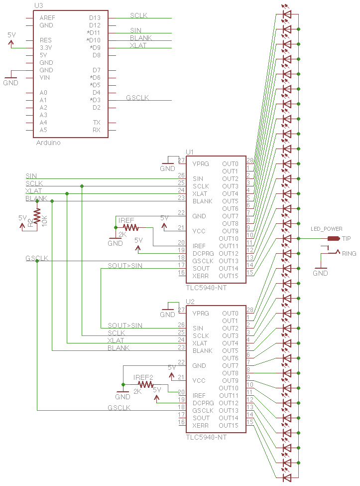
Look at pin 5 of the 1284 pinout. It is labeled "SS". That is the pin you use for the SS pin. (redefinable simply means you could change it to some other pin if you wanted to).
Did you install the TLC5940 Library ?
If you install it and look in the library folder, you will see a subdirectory named "Pinouts"
If you look in that subdirectory you will see all the pinout files for different Atmel processors.
One of them is named "ATmega_xx4.h".
If you had installed the Library you would have found this folder.
This is the contents of the file I am talking about that is installed with the library.
 /** \file
    SPI and timer pins for the ATmega164/324/644.  Don't edit these.  All
    changeable pins are defined in tlc_config.h */
T rust me I did go and look at the file. Which is why I am confused, I thought there would be a pin on the TLC5940 that you connect the ss pin and it didn't say in the library file where on the TLC5940 it is. but it seems once again I am wrong. Am I correct in saying this? So I just need to have ss pin defined in the library but I don't actually hook it up with the. TLC5940 right?
Did you install the TLC5940 Library ?
If you install it and look in the library folder, you will see a subdirectory named "Pinouts"
If you look in that subdirectory you will see all the pinout files for different Atmel processors.
One of them is named "ATmega_xx4.h".
If you had installed the Library you would have found this folder.
I have not install the library file instead I have looked at it using word wrap.
Still you have not installed the Library. I am trying to be patient but really this is difficult. You have to install the library to see the file (unless you use the zip file viewer). The ATmega_xx4.h contains a statement that reads this:
 /** \file
    SPI and timer pins for the ATmega164/324/644.  Don't edit these.  All
    changeable pins are defined in tlc_config.h */
I have attached the ATmega_xx4.h and the tlc_config.h file as well as Word text file copies of these two.
As you noticed, the pinouts file only mentions these:
SPI and timer pins for the ATmega164/324/644. (but NOT the 1284)
so I cannot say for certain that it will work. One thing is for sure , these files are part of the library. If you read my last post you know that the these files also mention the SS pin.
From the ATmega_xx4.h file in the Pinouts folder:
/** SS will be set to output as to not interfere with SPI master operation.
If you have changed the pin-outs and the library doesn't seem to work
or works intermittently, make sure this pin is set correctly. This pin
will not be used by the library other than setting its direction to
output. */
#define TLC_SS_PIN PB4
#define TLC_SS_DDR DDRB
Trust me I did go and look at the file. Which is why I am confused, I thought there would be a pin on the TLC5940 that you connect the ss pin and it didn't say in the library file where on the TLC5940 it is. but it seems once again I am wrong. Am I correct in saying this?
How can you look at the file if you didn't install the Library ? How can you look at the file I attached in the last post and not see this ?
/** SS will be set to output as to not interfere with SPI master operation.
If you have changed the pin-outs and the library doesn't seem to work
or works intermittently, make sure this pin is set correctly. This pin
will not be used by the library other than setting its direction to
output. */
#define TLC_SS_PIN PB4
#define TLC_SS_DDR DDRB
And now you are saying this?
So I just need to have ss pin defined in the library but I don't actually hook it up with the. TLC5940 right?
No. I am NOT saying that. I am saying AGAIN to drink 5 cups of coffee and read the ATmega_xx4.h file in the
PINOUTS folder. I attached this file to my last post. That file SPELLS OUT THE PINS TO USE FOR EVERYTHING. YOU NEED TO
CONNECT THOSE 1284 PINS (THE ONES IN THE ATmega1284PA-pinout.png image file. You read the ATmega_xx4.h file FIRST
THEN LOOK AT THE PINOUTS IMAGE FILE AND FIND THOSE PINS ON THE IMAGE FILE AND WRITE THOSE DOWN AND USE THOSE PINS . THE PINS IDENTIFIED ARE THE ONES YOU CONNECT AND THEIR PIN NAME IS SPECIFIED IT THE .h file. You write that pin name down , then look at the pinouts image file and you can see where those pins are. Those are the pins you connect .
Understand ?
ATmega_xx4.h (2.72 KB)
ATmega_xx4.txt (2.8 KB)
tlc_config.h (6.15 KB)