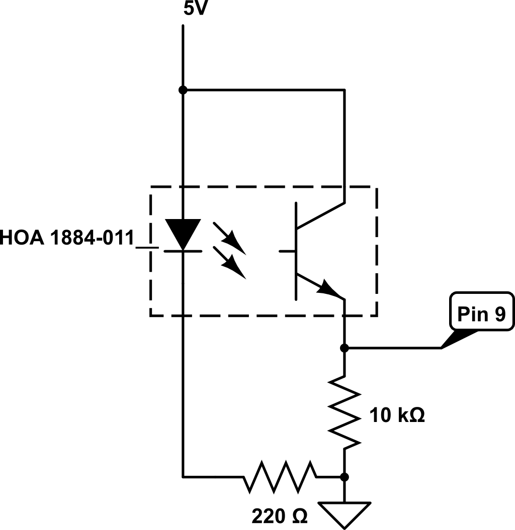
Ok, with a lot of reading and Googling, I got a photo interrupter to work last night (yay!). At the moment I am using an HOA 1884-012 wired up per the schematic below.
But it left me with three questions: (Let me know if I should have posted them individually.)
I can't really say I understand transistors, or much else about electronics for that matter, but using the schematic attached, I was able to write a sketch and see when the slot was interrupted. I have built a few circuits to learn about transistors, and those all apply a bit of voltage on the gate to get the current flow (please don't yell at me if that's the wrong way to express it) through the transistor, from collector to emitter (on an NPN, I think). All the "cartoon" images of a transistor show a big finger pushing on the gate to actuate it as a switch. So I'm expecting, with the IR LED shining, that it's "pushing" the gate, and when I Serial.print the pin state to pin 9, I'm going to see a HIGH when the slot is open, and a LOW when it is blocked. Imagine my surprise when it goes the other way!?!? What is going on here? Why is my mental model for this setup completely reversed?
My Googled examples used values for the collector-side resistor from 10k? to 100k?, but I never found an explanation of how to actually calculate a value for it. Looking at the datasheet, what characteristic of the phototransistor (or darlington) should I be looking at, and how would I determine a correct value if/when I pick another photo interrupter? In my trial-and-error experiments, it works with 10k? and 18k?, but quits working (doesn't change state) when I jump up to 100k?.
Referring back to #1, this is "acting" like a N.O. switch, for lack of a better way to describe that. For my application I really was envisioning using two of these, in series, as limit switches. If per my "mental model" above, of what I was expecting to happen, I thought they would act like N.C. switches and I'd be able to put two in series, and if either one opened, bingo, I'm done. Clearly not gonna work that way. So... what is the normal way to use two of these type devices in a limit-switch like application?
The LED is powered all the time. When it is able to shine on the transistor, the transistor is activated the same way as if current was being fed into the base. The light acts like base current. When the transistor switches on, it "pulls" the pin to ground which reads as LOW or 0. When you block the slot, the base current isn't applied so the transistor switches off and the pin is pulled high. You'll find allot of this kind of thing in electronics.
Used like this, you pick the resistor based upon how much power you can stand being "wasted" when it's on. You want to pick a value high enough that current actually flows; transistors have a cutoff current. With a 100k resistor, you would be limiting the current to a maximum of 50uA. This may be too low for the transistor to be able to turn on. A smaller resistor lowers the influence of electrical noise and possibly helps the transistor switch faster resulting in a nicer looking pulse.
In your case, the best approach may be to duplicate the circuitry and use two different pins to determine which switch was hit. You can't really just stack them up vertically.
I'm no expert but shouldn't that be wired along the lines of my pic below, which I know isn't the exact same sensor. It shows the pin connected to a divider on the transistor base.
@MarkT -- Duh, you're right, and I guess that's essentially the same as what afremont is suggesting with using a second pin, although his idea adds the benefit of seeing which one switched, at the cost of an additional pin.
@afremont -- Thank you for #1. That helps a lot. For #2, what parameter in the datasheet would I use? I don't see anything that helps me understand what criteria to use. And finally, thanks for the "second pin" suggestion. Clean and simple.
@JimboZA -- Your approach looks very similar, to me, if you consider your Input and Vcc to be coming from the same source, as the way mine is being used. Given what I understand now, your logic might be reversed though. I am not the expert as you can tell.
I may have spoke too soon. Now, I'm thinking that the 100k resistor combined with light leakage to the base allowed the transistor to turn on even when the slot was blocked. Try it again with the 100K resistor and measure the voltage at the collector to see if it is 5V or nearer to 0V. I'm thinking that you didn't detect any transitions because it was unable to pull the pin high after blocking the slot because the leakage drew too much current thru the 100k resistor.
It seems that I have been misinterpreting the collector-emitter cutoff parameter for a long time. This cutoff current is current that flows even with the base reverse biased. In other words it's leakage and will be present no matter what. With a big enough collector resistor, the leakage could be large enough to pull the collector low.
Your datasheet is quite lacking in specifics about the transistor used, but for the most part it really isn't important. You can see already that you can get it to work with a wide range of resistor values.
.... yes they are similar except mine has the pin measuring the output on the base edit: emitter, while yours is on the collector. But I have no idea if that's significant or not 8)
.... yes they are similar except mine has the pin measuring the output on the base, while yours is on the collector. But I have no idea if that's significant or not 8)
It is significant in that it results in the opposite polarity for the output. Doing it this way with a regular NPN transistor, you can run into problems turning the transistor all the way on though. As the transistor turns on and current flows, Rl will cause the emitter to start rising above ground potential and this will lead to less current flowing into the base. At some point an equilibrium will be reached, but it may not be a high enough voltage for the CPU to read it as a 1. Since this is a photo transistor, it's not a problem to get it turned all the way. I believe this to be correct.
I am away from my bench for the night now, but I will try the 100k and collector voltage reading in the morning to see what happens. I'll post back tomorrow.
.... yes they are similar except mine has the pin measuring the output on the base, while yours is on the collector. But I have no idea if that's significant or not 8)
I'm sure you meant emitter not base. The light input to the photo-transistor is the 'base' connection for the output transistor.
@afremont.... not sure which you're saying is correct?- taking the reading on the emitter side or the collector? (My pic is from a datasheet, so I'm guessing it's right....)
(As retrolefty pointed out, I obviously meant emitter not base in my earlier post)
Neither way is "correct" more than the other; it just depends upon what you want. The OP didn't like how it seemed reversed, doing it the way you showed would perhaps be more logical to him. In the OP's case, the reading is LOW when the transistor is on; in your circuit, the pin reading would be HIGH when the transistor is on (slot open).
I just wanted to point out that one might have problems using a "regular" NPN transistor in the manner of the circuit you posted since driving the base would become a challenge in many circuits. In the case of a photo-transistor it is not a problem, so either method may be used. I encourage the OP to try your method an see if he thinks the output to be more intuitive.
I believe that if you don't let the smoke out of something once in a while, you probably aren't learning as much as you could. See my signature line.
So spending a little time at the bench, and trying a few possibilities, here's what I found out:
The original version of my circuit, using a 10k? resistor seems like it works the best, but the 47k? would still reliably trip the pin, and "waste" less. The 100k? doesn't reliably switch the pin on.
I tried 2 variants on JimboZA's schematic, neither worked, nor triggered the transistor, nor successfully inverted the output. Both schematics attached, and in both approaches I had the anode of the LED and the collector of the transistor connected to 5V.
No magic smoke was emitted, and when returned to my original configuration, it still worked as before. Whew!
Schematics and results table attached.
Maybe I did something wrong or different than was suggested for testing?
In my defense/defence, my schematic was also from a data sheet, just not the one for the device I'm using/testing. Here is one example of why I chose to hook mine up the way I did... http://www.sparkfun.com/datasheets/PCB/PI-1120%20Breakout.pdf I scoured the web for application notes, schematics, datasheets and examples before trying this and posting.
I am ok with the output the way it is, I was just surprised, given my naive understanding of transistors, and what I thought should be happening. Hence my original question hoping someone would explain why. afremont's answer to #1 helps me understand what's going on.
I still don't know what characteristic in the datasheet would be used to calculate a correct value for the resistor.
All that said, I now see one more option I need to test...
Lest I be dinged for incompleteness of permutations, I realized I had to also test the variant where the resistor is still connected to the collector, but the pin/test node was on the emitter side... thinking that the resistor is still doing what it should, but by reading the other side of the transistor, the behavior might be inverted.
Nope. The photo-interrupter still trips, but the voltage at the pin stays the same all the time, ~4.94V.
I can see why #3 doesn't work, because the pin is forced to 5V. I do wonder why the pdf file of the test results doesn't show 5V present with the slot blocked or open. I would have expected #2 to work ok, but with reversed output.
EDIT: I just tested an NPN phototransistor with the collector tied to +5V, the emitter connected to an LED and then a resistor to ground. It worked exactly the same as when wired with LED and resistor between 5V and the collector and the emitter tied to ground.
Maybe you got the voltages reversed there? I also found that with the transistor on the "high side", I could only turn it on using the base pin connected to Vss (5V) to the point that I measured 3.85V at the emitter. Using actual light, I could turn the transistor on far enough to get the emitter to 4.4V. My Vss measures out at 5.1V.
I see you just posted again, so I'll get that question now. Just pick a value that you like the characteristics of. These characteristics being how much power can you tolerate to burn and how fast you need your rise/fall times to be.