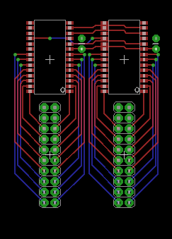
10 mil (0.010 inch) traces on 25 mil (0.025 inch) centers with 13 mil (0.013 inch ) vias. (I'll leave it to you to figure the metric equivalents.)
Well within the abilities of a board house like OSHpark without hitting the limits (except for vias which are right at the limit - I prefer vias a little bigger at 20 mil, but they take up more room and don't fit between 25 mil trace spacing.)
You will, of course, need to use minimum sizes that correlate to your board house's abilities, but there is at least one house out there that can handle it.
leen15:
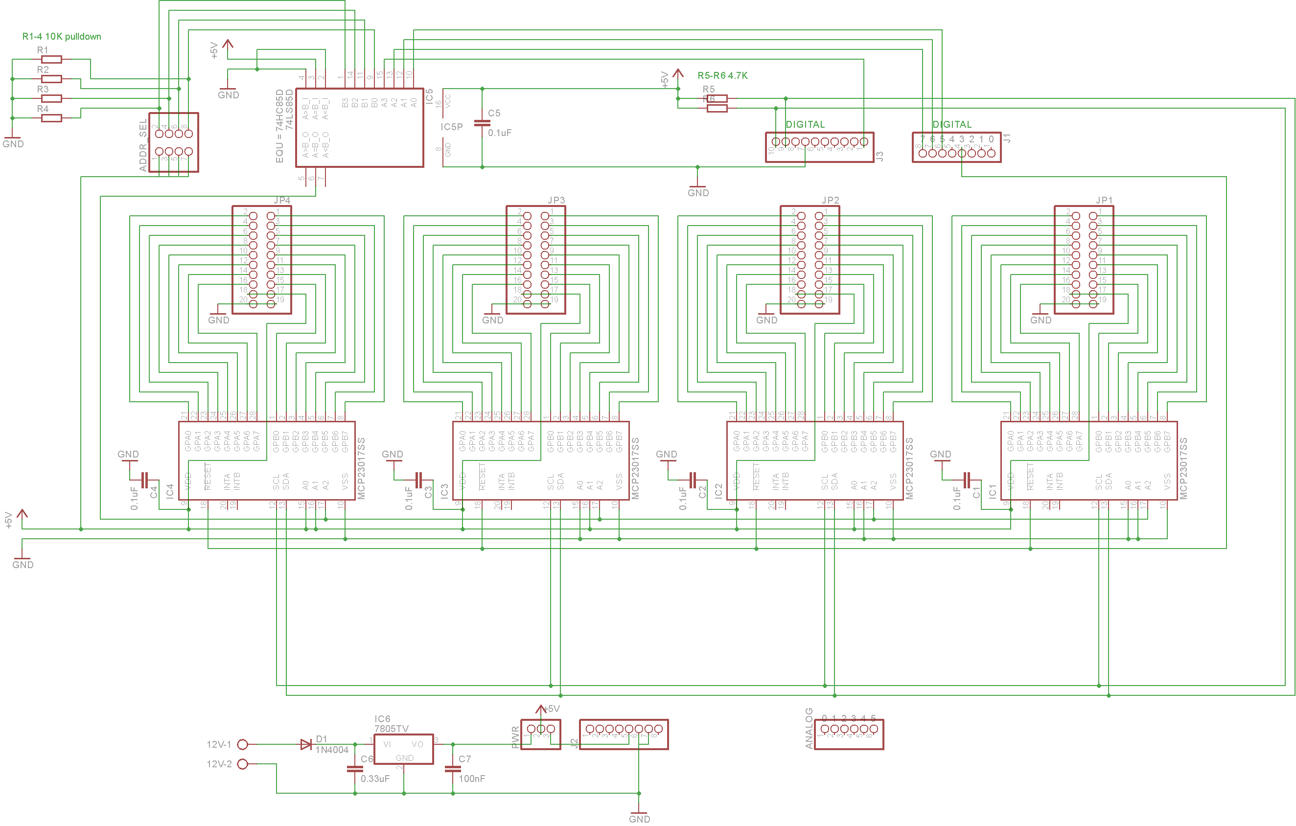
This is what I've done until now.
A good start! I like how you used the heavy traces for power. But you need to keep them heavy between the connectors as well. Also, use heavier traces to power the chips, especially between the bypass caps and the chips. It's going to be tough to get power and ground to the connector power pins, because those parallel top and bottom traces act as impenetrable barriers (unless you go to four layers and add power and ground planes.) it would be better to put the power pins on the other end of the connectors, that way you can run a heavy bus right down the row.
Sometimes, you can't do the perfect pin ordering on connectors, and sometimes you could but it's not worth the effort. If you put the power pins on the opposite end, it may not line up directly with a relay board: bit 0 goes to 7, 1 to 6, 2 to 5, and so on. Not ideal, but you can work around that in software with a pin translation lookup table. (Or just put stickers on the relay board with the correct logical PIN number!)
Another thing to watch out for are "acid traps" which is where a trace intersection forms a tight acute angle. Take a look at how the SCL trace leaves the header pad. It forms a tight narrow corner that can trap acid during the etching process and eat away too much of the trace (or something like that, I don't know the details, just that it's a bad idea.) compare it to the SDA trace, and toy can see where that little bit of vertical offset has it leaving the pad almost perpendicularly. Oval pads can make soldering easier, especially on long leads, but I prefer round or octagonal pads because you don't have to worry about departure angle so much.
I didn't use autoroute, i prefered to do it manually.
Autoroute is horrible, you are wise to stay away from it. I clicked it once to see what it would do with a simple layout, and it was really ugly. I'm sure it won't handle this board, it would just lay out a bunch of meandering random traces, and then give up, leaving you no room to do the rest.
Besides, I like manually routing: I find it relaxing and a fun puzzle to solve.
The problem is that DRC tells me that i've too little space between wires, too little width of wires and too little drill size. 
Are you using the default DRC rules? The minimum sizes and spaces they use are pretty big. You need to choose the board house that will make the boards, and get the minimum parameters from them. Things like minimum trace width, trace spacing, via sizes, clearances, etc. Many board houses will have Eagle rules files you can download and load directly, others you will have to enter manually (and if that's the case, make sure to save then to a settings file for later use.)
What is the min size of wires and vias for no DRC errors?
It depends. The better the board house and the processes they use, the finer work they can do, and the smaller values you can use. Go cheap, and their limits will often be bigger. If you plan on etching the board yourself, then you probably want to increase the size of the default limits. (This board is complex enough that I don't think home etching is going to be practical.)
This is already too much typing to do on a tablet. I'll take another look at this when I get to my computer and see if I see anything else.