We have sifted through all the posts I could find on various relevant topics to try to collect all gotchas (e.g., errors in Schematics, suboptimal I2C pullup resistor values). We have also looked for various types of user feedback to help us design a board that can not only be useful for us but also could be interesting for others making small production runs based on SAM3X8E. E.g. we have added a 64Kbit EEPROM on board, broken out AREF pin, etc.
At this moment, we were able to get a 4-layer layout containing LQFP-144 package to fit into a 1.2"x1.4" footprint. It would have an external programming board with Due programming circuit on it. This way small production runs are way more economical as you don't have to spend all that $$ and board space on programmer circuits you don't use in production.
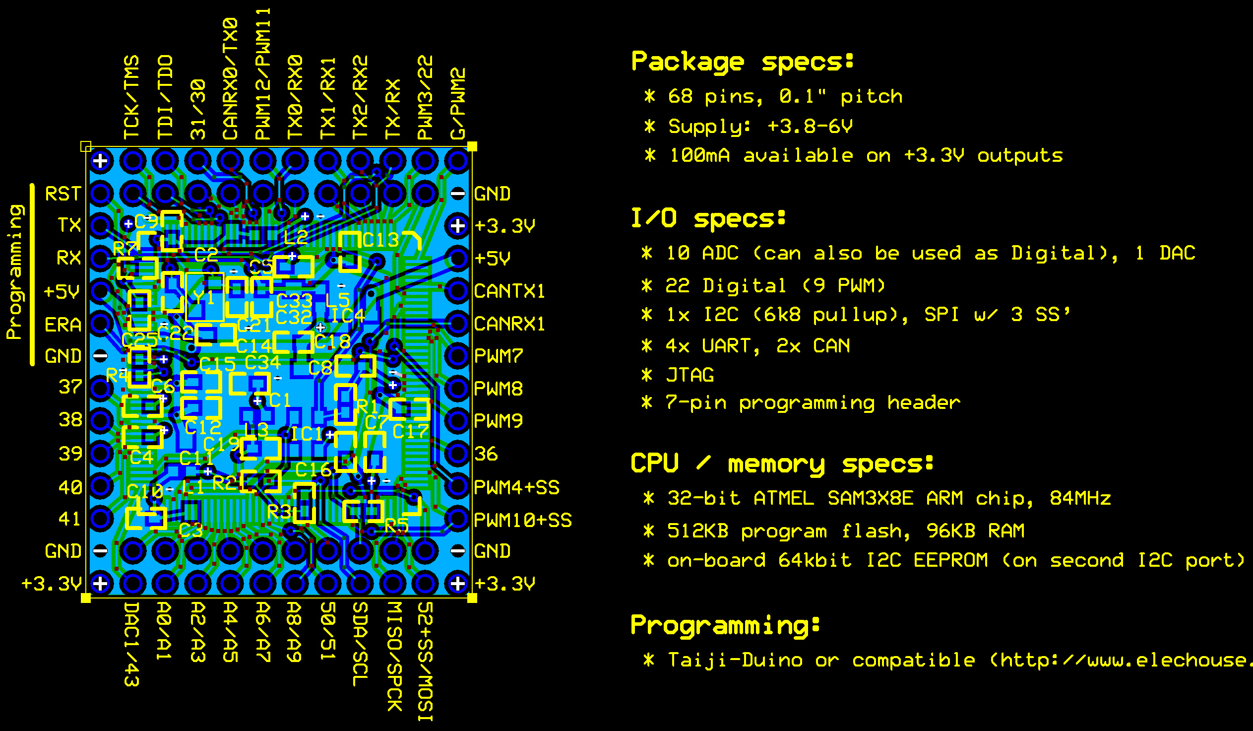
See the screenshot below for some details. The picture is admittedly a bit messy with all layers visible - SAM chip is mounted on top of board, all other components - on the bottom. 68 .1" pins on perimeter. Main design objective was the smallest footprint while maximizing the number of peripheral types broken out. The trade-off is a smaller number of broken-out Digital I/O pins. You will also notice there are no reset / erase buttons. Again, we do not expect those to be useful in production environment. And they would take a huge amount of space + cost of electromech components is non-trivial.
In addition to general feedback, would be cool to hear your opinion on some open questions we still have:
What should we do with VBUS / UOTGVBOF / VBG lines? We are NOT breaking out Native USB at this point so none of the USB hardware would actually be used but I am wondering what we need to keep from the original Due schematics so the system still works. E.g., should we provide VCC to VBUS input? Should we still have an RC network on VBG pin? Etc.
Should we try to break out native USB? The reason it's not on right now is that a micro-AB slot would take 20% of our board space and in fact would make the board at least 40% larger. Soon enough the space benefit from having this MicroDue board is diminished. So unless one can see extremely high utility for native USB, we would keep it out. IMO given that there is going to be a separate programmer board, native USB is ONLY useful for USB HOST mode. I am just not sure what % of target users this will be important for. Maybe I am missing some uses other than USB HOST?
Are there any other gotchas we should be aware of?
make the USB port available just as pins (DHSDP, DFSDP, DHSDM, DFSDM, UOTGID, USBVCC) so it is possible to create a small shield with an USB adapter for those, who need it.
If you can include the neglected slave select pin NPCS3 (LFBGA pin A2) for SPI, then it would be possible to use the external decoder support to allow up to 15 peripherals. That one wire could expand SPI peripherals to 4 (or 15 with decoder). It looks like the Arduino software already supports this pin, but its left unconnected on the Due board.
Nice mini-board - I was (am) considering something similar - a mini core board with LFBGA that breaks out all pins.
Good idea on adding usb pins. Would you want the associated circuitry on this board or leave out for the shield?
Depending on space. The most important point would be, to have the pins available. If there is space left on the board for the circuitry, the shield would be very easy. Without pins however, the functions are not accessible.
Better leave the circuitry off, if that gives you space for other pins.
Cost wise I expect $13 all in. Assuming good volume of course
I assume, that this should be no problem with a good crowdfunding campaign.
thx. added a row of pins to break this out. circuitry on board so you just need to connect the pins to VUSB, D+, D-, ID, UGND. I wonder if there are some creative ways to simplify addition of the connector to these...
Used some extra space to add 4 additional digital pins and better layout for AREF reference.
got it. but why would this need to be broken out? why not leave it permanently tied to +3.3V supply?
What might need to be broken out is RTC crystal pads, right? I mean, if we go to the trouble of breaking out NRST, we should make RTC fully functional, right?
valerun:
got it. but why would this need to be broken out? why not leave it permanently tied to +3.3V supply?
Figure 5-3 in the Atmel-Dokumentation shows the purpose, when you wish to connect the backup-batterie like a small coin package. That may need some kind of solder-pad, where the connection to +3.3V can be cutted/solder-closed as needed.
valerun:
What might need to be broken out is RTC crystal pads, right? I mean, if we go to the trouble of breaking out NRST, we should make RTC fully functional, right?
Right with that, but the second advantage is, that the NRST is bidirectional, so that external components can be reset through it.
If you connect the external components to NRST they are reset, whenever the reset-controller resets the chip, even when caused by software! That means, that you need no code, which uses GPIO-pins to reset your peripherals.
valerun:
got it. but why would this need to be broken out? why not leave it permanently tied to +3.3V supply?
Figure 5-3 in the Atmel-Dokumentation shows the purpose, when you wish to connect the backup-batterie like a small coin package. That may need some kind of solder-pad, where the connection to +3.3V can be cutted/solder-closed as needed.
Thanks. I read through that section but can't understand if there is going to be any residual consumption on rest of VDD pins if the chip is put into a backup mode... If the consumption is zero on all other pins (chip is down, after all), then one could just keep the battery connected to all supply pins at all times. This does assume that the user would move the chip to backup mode once loss of 3.3v external power is detected (perhaps using one of the digital pins to sense that). But this does sound like a kludge. Will try to break this one out, as well. Running out of space, though
The SAM has a SHDN pin that is supposed to be used to shut down external regulators, that may imply that this should be done to get the best low power operation, but I think it's just to kill external circuitry, the CPU itself has this well handled.
One would assume as you say that the current used on the VDD pins is next to nothing, in fact if you look at Fig 46-4 they have all the VDD pins shorted to GND for testing the VDDBU current, so it's fair to say there is nothing but some leakage current on those pins under a normal shutdown situation.
ok got the USB pins out (R5, R6 39R resistors fitted on board but varistors don't fit so a shield would have to implement those).
Also got the VDDBU out (bridged to +3.3v - would need to be cut if this feature is used).
Finally, was able to fit in 32khz crystal and caps - at the expense of one digital pin breakout I just would hate to have sensitive crystal circuitry broken out via huge 0.1" pins...
All this cost ~8% increase in board size. On the plus side, that allowed adding one more analog and a few digital pins
added one more row on the 109-144 side of the chip which allowed a few additional digital pins but more importantly placing a 3.3v CAN tranceiver to be able to use an excellent CAN-DUE library by collins80 and a few others. These tranceivers run in our EV chargers and work like a charm. So now we have a fully plug-and-play CAN channel on board.
1.4"x1.4" board with 91 pins in 2 rows along the perimeter. The original idea was to have ~40 pins... lol
Sample chips arrived from ATMEL today.
Any other suggestions before we order the first ~10 boards for testing?
That really sounds like a boost-board for the DUE-family. A fraction of the size of the original, with an estimated price, where you have not to think about letting the board in a project.
someone mentioned something about breaking out EBI data bus... What do you guys think about that? Better be very critical as I REALLY don't want to add a third row of pins