SAMD51 TC PWP mode for measuring frequency - Inputs?

Hello!

I would like to try and use a ATSAMD51J to read 4 distinct digital inputs, duty cycle and period. I've been reading around and think the TC instances should be able to do this, but wanted to ask to be sure.

I would like to measure 4 frequencies from around 0Hz to 100KHz, and I would like to measure the duty cycle too if possible. I would like to store this info in a 16bit integer representing a final resolution of 0.01ms, and I'd like to be able to let the counter overflow once before letting the input "stall" as well, so a final output resolution of 17bits. I think I can use the overflow and capture interrupts enables to manage this.

If I set up a TC instance with a Gclk/prescale that gets me a 100KHz clock, plus figuring out the pinmux to make sure the WO signal gets where it needs to go (as well as all the other timer register configs) will it work as I'm expecting? From there, can I use the overflow interrupt to force four independent ISRs that will let me track overflows?

Can interrupts stack, at least till they are serviced, so that I might just loose a bit of measurement accuracy at those extremely slow input frequencies? (4x potential interrupts at ~1.5Hz) And running all 4 frequency inputs as separate timer inputs instead of ISR triggered events is probably the best way to prevent much larger inaccuracies at higher input frequencies, or am I missing something?

And I keep reading about the inability to map TC WO channels and using events instead, is that a SAMD21 thing, or is atmel start and datasheets lying to me?

Thank you for your time!

Hi microsootys,

Yes, I think it's probably possible, but capturing pulse width and period at 100kHz on 4 inputs, contains a lot of information in a short period of time.

How you implement measuring the pulse width and period, depends upon what you intend to do with this information?

For example, if you intend to just to occasionally take a single reading of the incoming data, then this could be implemented using interrupts. If on the other hand, you need take consecutive samples, say to store waveform to an SD card, then the Direct Memory Access using the DMAC is the way to go.

In any case, the input pins are connected to the TC/TCC timers via the EIC (External Interrupt Controller) and the event system (a 32-channel peripheral-to-peripheral highway). This allows a signal on almost any external IO pin on the microcontroller to be fed through to any timer. The timers themselves are set to PPW or PWP mode with the data being captured in the timers' CC0 and CC1 registers. These registers can be read either using interrupts or the DMAC, depending on your project's requirements.

I intend to send the latest output data over i2c once every 50-100ms, maybe with a little averaging in the middle. I plan on leaving the capture interrupt disabled the majority of the time, maybe only turning it on after the first overflow then using it to reset my external overflow flag followed by turning it back off once a new result is available. I still need to do a few other minor things with the CPU, so leaving it alone to only service these 4 inputs won't work.

Would it not be better to just use the peripheral pins directly instead of the EIC and event system? I am talking about section 6.2.8.4 of the datasheet, the WO0/1 pins each TC instance has. I don't understand why you would use the EIC and event system otherwise, assuming the pins needed are available?

Thank you!!

Hi microsootys,

Yes, as you mention it looks like the SAMD51, (unlike the SAMD21), has the option to activate its TC timer pins as inputs.

However, the explanation in the SAMD51 datasheet is so poor, being just a couple of sentences bolted on to what is essentially a cut 'n' paste job from the SAMD21 datasheet, that it's currently not clear (to me at least) how it's intended to work. Maybe it will become clearer after some experimentation?

Anyway for now, here's an example for the Adafruit Feather M4, using the EIC and event system. It generates a test, 100kHz PWM signal using timer TCC0, alternating between 25% and 75% duty-cycles on digital pin D10. This can be plugged into input on analog pin A4 that is routed to timer TC0 (not TCC0) via the EIC and event system.

The code triggers two TC0 interrupts every second, one to read the pulsewidth and the other the period. The results are displayed on the console:

// Adafruit Feather M4: Setup TC0 to count pulse width and period on analog pin A4
// 100kHz test frequency on digtial pin D10

volatile uint16_t period;
volatile uint16_t pulsewidth;

void setup()
{
  Serial.begin(115200);                              // Open the serial port at 115200 baud
  while(!Serial);                                    // Wait for the console to open
 
  MCLK->APBBMASK.reg |= MCLK_APBBMASK_EVSYS;         // Switch on the event system peripheral
  
  // Set up the generic clock (GCLK7) used to clock timers 
  GCLK->GENCTRL[7].reg = GCLK_GENCTRL_DIV(1) |       // Divide the 120MHz clock source by divisor 1: 120MHz/1 = 120MHz
                         GCLK_GENCTRL_IDC |          // Set the duty cycle to 50/50 HIGH/LOW
                         GCLK_GENCTRL_GENEN |        // Enable GCLK7
                         //GCLK_GENCTRL_SRC_DFLL;      // Generate from 48MHz DFLL clock source
                         GCLK_GENCTRL_SRC_DPLL0;     // Generate from 120MHz DPLL clock source
                         //GCLK_GENCTRL_SRC_DFLL1;     // Generate from 100MHz DPLL clock source
  while (GCLK->SYNCBUSY.bit.GENCTRL7);               // Wait for synchronization
  
  GCLK->PCHCTRL[TC0_GCLK_ID].reg = GCLK_PCHCTRL_CHEN |         // Enable perhipheral TC0
                                   GCLK_PCHCTRL_GEN_GCLK7;     // Connect  120MHz generic clock 7 to TC0

  GCLK->PCHCTRL[TCC0_GCLK_ID].reg = GCLK_PCHCTRL_CHEN |        // Enable perhipheral TCC0
                                    GCLK_PCHCTRL_GEN_GCLK7;    // Connect  120MHz generic clock 7 to TCC0
                                  
  // Enable the peripheral multiplexer on pin D10
  PORT->Group[g_APinDescription[10].ulPort].PINCFG[g_APinDescription[10].ulPin].bit.PMUXEN = 1;
  
  // Set the D10 (PORT_PA20) peripheral multiplexer to peripheral (even port number) G(6): TCC0, Channel 0
  PORT->Group[g_APinDescription[10].ulPort].PMUX[g_APinDescription[10].ulPin >> 1].reg |= PORT_PMUX_PMUXE(MUX_PA20G_TCC0_WO0);             
  
  TCC0->WAVE.reg = TCC_WAVE_CICCEN0 |                // Set-up TCC0 to alternate duty-cycle between CC0 and CCBUF0 registers
                   TCC_WAVE_WAVEGEN_NPWM;            // Set-up TCC0 timer for Normal (single slope) PWM mode (NPWM)
  while (TCC0->SYNCBUSY.bit.WAVE);                   // Wait for synchronization

  TCC0->PER.reg = 1199;                              // Set-up the PER (period) register for 100KHz output
  while (TCC0->SYNCBUSY.bit.PER);                    // Wait for synchronization
  
  TCC0->CC[0].reg = 300;                             // Set-up 25% duty-cycle
  while (TCC0->SYNCBUSY.bit.CC0);                    // Wait for synchronization

  TCC0->CCBUF[0].reg = 900;                          // Set-up 75% duty-cycle
  
  TCC0->CTRLA.bit.ENABLE = 1;                        // Enable timer TCC0
  while (TCC0->SYNCBUSY.bit.ENABLE);                 // Wait for synchronization
  
  // Enable the port multiplexer on analog pin A4
  PORT->Group[g_APinDescription[A4].ulPort].PINCFG[g_APinDescription[A4].ulPin].bit.PMUXEN = 1;
 
  // Set-up the pin as an EIC (interrupt) peripheral on analog pin A4
  PORT->Group[g_APinDescription[A4].ulPort].PMUX[g_APinDescription[A4].ulPin >> 1].reg |= PORT_PMUX_PMUXE(MUX_PA04A_EIC_EXTINT4);

  EIC->CTRLA.bit.ENABLE = 0;                        // Disable the EIC peripheral
  while (EIC->SYNCBUSY.bit.ENABLE);                 // Wait for synchronization 
  EIC->CONFIG[0].reg = EIC_CONFIG_SENSE4_HIGH;      // Set event on detecting a HIGH level
  EIC->EVCTRL.reg = 1 << 4;                         // Enable event output on external interrupt 4 
  EIC->INTENCLR.reg = 1 << 4;                       // Clear interrupt on external interrupt 4
  EIC->ASYNCH.reg = 1 << 4;                         // Set-up interrupt as asynchronous input
  EIC->CTRLA.bit.ENABLE = 1;                        // Enable the EIC peripheral
  while (EIC->SYNCBUSY.bit.ENABLE);                 // Wait for synchronization
 
  // Select the event system user on channel 0 (USER number = channel number + 1)
  EVSYS->USER[EVSYS_ID_USER_TC0_EVU].reg = EVSYS_USER_CHANNEL(1);                   // Set the event user (receiver) as timer TC0 

  // Select the event system generator on channel 0
  EVSYS->Channel[0].CHANNEL.reg = EVSYS_CHANNEL_EDGSEL_NO_EVT_OUTPUT |              // No event edge detection
                                  EVSYS_CHANNEL_PATH_ASYNCHRONOUS |                 // Set event path as asynchronous
                                  EVSYS_CHANNEL_EVGEN(EVSYS_ID_GEN_EIC_EXTINT_4);   // Set event generator (sender) as external interrupt 4 

  TC0->COUNT16.EVCTRL.reg = TC_EVCTRL_TCEI |                // Enable the TCC event input
                            //TC_EVCTRL_TCINV |             // Invert the event input         
                            TC_EVCTRL_EVACT_PPW;            // Set up the timer for capture: CC0 period, CC1 pulsewidth

  NVIC_SetPriority(TC0_IRQn, 0);      // Set the Nested Vector Interrupt Controller (NVIC) priority for TC0 to 0 (highest)
  NVIC_EnableIRQ(TC0_IRQn);           // Connect the TC0 timer to the Nested Vector Interrupt Controller (NVIC)

  TC0->COUNT16.INTENSET.reg = TC_INTENSET_MC1 |             // Enable compare channel 1 (CC1) interrupts
                              TC_INTENSET_MC0;              // Enable compare channel 0 (CC0) interrupts 
                                      
  TC0->COUNT16.CTRLA.reg = TC_CTRLA_CAPTEN1 |               // Enable pulse capture on CC1
                           TC_CTRLA_CAPTEN0 |               // Enable pulse capture on CC0
                           //TC_CTRLA_PRESCSYNC_PRESC |     // Roll over on prescaler clock
                           //TC_CTRLA_PRESCALER_DIV1 |      // Set the prescaler
                           TC_CTRLA_MODE_COUNT16;           // Set the timer to 16-bit mode
  
  TC0->COUNT16.CTRLA.bit.ENABLE = 1;                        // Enable the TC0 timer
  while (TC0->COUNT16.SYNCBUSY.bit.ENABLE);                 // Wait for synchronization
}

void loop()
{  
  TC0->COUNT16.INTENSET.reg = TC_INTENSET_MC1 |             // Enable compare channel 1 (CC1) interrupts
                              TC_INTENSET_MC0;              // Enable compare channel 0 (CC0) interrupts 
  while (TC0->COUNT16.INTENSET.bit.MC1 ||                   // Wait for the pulse width and period to be read 
         TC0->COUNT16.INTENSET.bit.MC0);                   
  Serial.print(pulsewidth);                                 // Output the results
  Serial.print(F("   ")); 
  Serial.println(period); 
  delay(1000);                                              // Wait for 1 second                               
}

void TC0_Handler()                                          // Interrupt Service Routine (ISR) for timer TC0
{      
  if (TC0->COUNT16.INTFLAG.bit.MC0)                         // Check for match counter 0 (MC0) interrupt
  {   
    period = TC0->COUNT16.CC[0].reg;                        // Copy the period 
    TC0->COUNT16.INTENCLR.reg = TC_INTENCLR_MC0;            // Disable compare channel 0 (CC0) interrupts                            
  }
 
  if (TC0->COUNT16.INTFLAG.bit.MC1)                         // Check for match counter 1 (MC1) interrupt
  {
    pulsewidth = TC0->COUNT16.CC[1].reg;                    // Copy the pulse width 
    TC0->COUNT16.INTENCLR.reg = TC_INTENCLR_MC1;            // Disable compare channel 1 (CC1) interrupts                               
  }
}

Thank you for the example!

I will play with the W/O inputs and see if I can make them work without using the EIC or Event system. I wish I understood how they worked better. If everything is set up asynchronous, will one EIC or event ever block or delay another? And if so, would using the W/O pins prevent that?

It seems the PWP selection is under the event control register, and the datasheet bounces between using signal and event for describing the PWP input. I guess it's possible it's just ripped from the older datasheet of the SAMD21 which didn't have W/O inputs?

I will see what I can come up with and share! I currently have a ATSAME51 custom board I made working in arduino with all I/O exposed, so getting to the W/O pins shouldn't be a problem.

Hi microsootys,

The event system has to be set for asynchronous operation when routing signals to the TC timers.

The event system will not block and is extremely fast, although the asynchronous signal do incur a small delay of a few clock cycles passing through the EIC.

It's necessary to use a new event channel for each of your other inputs. The SAMD51/SAME51 has 32 event channels in total.

As you mention, it seems like the TC timers PWP mode is tied up with the event system.

The code I posted is just a template and you might have to change the TC prescaler and/or the GCLK divider, to get the correct frequency range.

I've also got an example that uses the DMAC as well, if you require it?

I think I may have found the older samd21 TCC thread, towards the end there were examples (From you again, thank you!) for DMA. Closest I think I've ever been to understanding it, I've got stuck in DMA interrupts whenever I try using it myself at the moment...

A common sized error in timing wouldn't be the end of the world, but if the error were dependent on how many inputs are currently synchronized would be more of an issue. For what I am after and at these clock frequencies I'm not sure I'd even try to calibrate the consistent timing errors out.

I think I can manage to look through the DFU packs from atmel to figure out how to reference all those things for adding more pins. But, if that example is handy I wouldn't mind taking a look!

I also think I can figure out the Gclk and prescaler. I wrote a bit of code for the canbus timings on the same51 that will try different gclk sources and peripheral prescalers to try and target an evenly divided fixed sample point and baudrate that seems to work ok. I think the TC will be similar, if not a lot easier! I think I've read before that some timers share a gclk, but can use different prescalers? I think they are tied in pairs, right? TC0/TC1 are shared, same with TC2/TC3, TC4/TC5, TC6/TC7. Only TCC4 is on it's own, I guess with pairing for 32bit possible that makes sense. No matter in my case, 4 of them will share a common gclk anyway.

Thank you again for your help, now and in the past!

Hi microsootys,

I had a look on the internet to see if others had encountered the same problem with TC inputs. Turns out that others have had similar issue with the SAMC21: https://www.avrfreaks.net/forum/samc21-cannot-use-tc-capture-inputs-ppw-or-pw-modes.

Unfortuately, I currently can't find the solution, other than using the EIC and event system.

Here's the code using the DMAC, it continuously captures pulse width and period measurements, it uses the same pins, D10 for test output, A4 for input:

// Adafruit Feather M4: Setup TC0 to capture pulse-width and period at up to 100kHz
uint16_t dmacPeriod;
uint16_t dmacPulsewidth;

typedef struct                              // DMAC descriptor structure
{
  uint16_t btctrl;
  uint16_t btcnt;
  uint32_t srcaddr;
  uint32_t dstaddr;
  uint32_t descaddr;
} dmacdescriptor ;

volatile dmacdescriptor wrb[DMAC_CH_NUM] __attribute__ ((aligned (16)));               // Write-back DMAC descriptors
dmacdescriptor descriptor_section[DMAC_CH_NUM] __attribute__ ((aligned (16)));         // DMAC channel descriptors
dmacdescriptor descriptor __attribute__ ((aligned (16)));                     // Place holder descriptor

void setup()
{
  Serial.begin(115200);                  // Send data back on the Zero's native port
  while(!Serial);                        // Wait for the Serial port to be ready
  
  DMAC->BASEADDR.reg = (uint32_t)descriptor_section;                // Set the descriptor section base address
  DMAC->WRBADDR.reg = (uint32_t)wrb;                                // Set the write-back descriptor base adddress
  DMAC->CTRL.reg = DMAC_CTRL_DMAENABLE | DMAC_CTRL_LVLEN(0xf);      // Enable the DMAC and priority levels
 
  // Set DMAC channel 0 to trigger on TC0 match compare 1 and to trigger every beat
  DMAC->Channel[0].CHCTRLA.reg = DMAC_CHCTRLA_TRIGSRC(TC0_DMAC_ID_MC_0) | DMAC_CHCTRLA_TRIGACT_BURST;
  descriptor.descaddr = (uint32_t)&descriptor_section[0];           // Set up a circular descriptor
  descriptor.srcaddr = (uint32_t)&TC0->COUNT16.CC[0].reg;           // Take the contents of the TC0 counter comapare 0 register
  descriptor.dstaddr = (uint32_t)&dmacPeriod;                       // Copy it to the "dmacPeriod" variable
  descriptor.btcnt = 1;                                             // This takes one beat
  descriptor.btctrl = DMAC_BTCTRL_BEATSIZE_HWORD | DMAC_BTCTRL_VALID;   // Copy 16-bits (HWORD) and flag discriptor as valid
  memcpy(&descriptor_section[0], &descriptor, sizeof(dmacdescriptor));  // Copy to the channel 0 descriptor
                     
  // Set DMAC channel 1 to trigger on TC0 match compare 1 and to trigger every beat
  DMAC->Channel[1].CHCTRLA.reg = DMAC_CHCTRLA_TRIGSRC(TC0_DMAC_ID_MC_1) | DMAC_CHCTRLA_TRIGACT_BURST;
  descriptor.descaddr = (uint32_t)&descriptor_section[1];           // Set up a circular descriptor
  descriptor.srcaddr = (uint32_t)&TC0->COUNT16.CC[1].reg;           // Take the contents of the TC0 counter comapare 1 register
  descriptor.dstaddr = (uint32_t)&dmacPulsewidth;                   // Copy it to the "dmacPulseWidth" variable
  descriptor.btcnt = 1;                                             // This takes 1 beat
  descriptor.btctrl = DMAC_BTCTRL_BEATSIZE_HWORD | DMAC_BTCTRL_VALID;    // Copy 16-bits (HWORD) and flag discriptor as valid
  memcpy(&descriptor_section[1], &descriptor, sizeof(dmacdescriptor));   // Copy to the channel 1 descriptor 

  GCLK->PCHCTRL[TCC0_GCLK_ID].reg = GCLK_PCHCTRL_CHEN |        // Enable the TCC1 perhipheral channel
                                    GCLK_PCHCTRL_GEN_GCLK0;    // Connect 120MHz generic clock 0 to TCC0
  
  // Enable the peripheral multiplexer on pin D10
  PORT->Group[g_APinDescription[10].ulPort].PINCFG[g_APinDescription[10].ulPin].bit.PMUXEN = 1;
  
  // Set the D10 (PORT_PA20) peripheral multiplexer to peripheral (even port number) G(6): TCC0, Channel 0
  PORT->Group[g_APinDescription[10].ulPort].PMUX[g_APinDescription[10].ulPin >> 1].reg |= PORT_PMUX_PMUXE(MUX_PA20G_TCC0_WO0);             
  
  TCC0->WAVE.reg = TCC_WAVE_CICCEN0 |                // Set-up TCC0 to alternate duty-cycle between CC0 and CCBUF0 registers
                   TCC_WAVE_WAVEGEN_NPWM;            // Set-up TCC0 timer for Normal (single slope) PWM mode (NPWM)
  while (TCC0->SYNCBUSY.bit.WAVE);                   // Wait for synchronization

  TCC0->PER.reg = 1199;                              // Set-up the PER (period) register for 100KHz output
  while (TCC0->SYNCBUSY.bit.PER);                    // Wait for synchronization
  
  TCC0->CC[0].reg = 300;                             // Set-up 25% duty-cycle
  while (TCC0->SYNCBUSY.bit.CC0);                    // Wait for synchronization

  TCC0->CCBUF[0].reg = 900;                          // Set-up 75% duty-cycle
  
  TCC0->CTRLA.bit.ENABLE = 1;                        // Enable timer TCC0
  while (TCC0->SYNCBUSY.bit.ENABLE);                 // Wait for synchronization

  MCLK->APBBMASK.reg |= MCLK_APBBMASK_EVSYS;         // Switch on the event system peripheral
 
  GCLK->PCHCTRL[TC0_GCLK_ID].reg = GCLK_PCHCTRL_CHEN |         // Enable perhipheral channel
                                   GCLK_PCHCTRL_GEN_GCLK0;     // Connect 120MHz generic clock 0 to TC0
  
  // Enable the port multiplexer on analog pin A4
  PORT->Group[g_APinDescription[A4].ulPort].PINCFG[g_APinDescription[A4].ulPin].bit.PMUXEN = 1;
 
  // Set-up the pin as an EIC (interrupt) peripheral on analog pin A4
  PORT->Group[g_APinDescription[A4].ulPort].PMUX[g_APinDescription[A4].ulPin >> 1].reg |= PORT_PMUX_PMUXE(0);//(MUX_PA04A_EIC_EXTINT4);
  
  EIC->CTRLA.bit.ENABLE = 0;                        // Disable the EIC peripheral
  while (EIC->SYNCBUSY.bit.ENABLE);                 // Wait for synchronization 
  EIC->CONFIG[0].reg = EIC_CONFIG_SENSE4_HIGH;      // Set event on detecting a HIGH level
  EIC->EVCTRL.reg = 1 << 4;                         // Enable event output on external interrupt 4 
  EIC->INTENCLR.reg = 1 << 4;                       // Clear interrupt on external interrupt 4
  EIC->ASYNCH.reg = 1 << 4;                         // Set-up interrupt as asynchronous input
  EIC->CTRLA.bit.ENABLE = 1;                        // Enable the EIC peripheral
  while (EIC->SYNCBUSY.bit.ENABLE);                 // Wait for synchronization
 
  // Select the event system user on channel 0 (USER number = channel number + 1)
  EVSYS->USER[EVSYS_ID_USER_TC0_EVU].reg = EVSYS_USER_CHANNEL(1);         // Set the event user (receiver) as timer TC0 

  // Select the event system generator on channel 0
  EVSYS->Channel[0].CHANNEL.reg = EVSYS_CHANNEL_EDGSEL_NO_EVT_OUTPUT |              // No event edge detection
                                  EVSYS_CHANNEL_PATH_ASYNCHRONOUS |                 // Set event path as asynchronous
                                  EVSYS_CHANNEL_EVGEN(EVSYS_ID_GEN_EIC_EXTINT_4);   // Set event generator (sender) as external interrupt 4 

  TC0->COUNT16.EVCTRL.reg = TC_EVCTRL_TCEI |                // Enable the TCC event input
                            //TC_EVCTRL_TCINV |               // Invert the event input         
                            TC_EVCTRL_EVACT_PPW;            // Set up the timer for capture: CC0 period, CC1 pulsewidth
                                     
  TC0->COUNT16.CTRLA.reg = TC_CTRLA_CAPTEN1 |               // Enable capture on CC1
                           TC_CTRLA_CAPTEN0;// |            // Enable capture on CC0
                           //TC_CTRLA_PRESCALER_DIV1 |        // Set prescaler to 1
                           //TC_CTRLA_PRESCSYNC_PRESC;        // Timer to wrap around on next prescaler clock                   
                            
  TC0->COUNT16.CTRLA.bit.ENABLE = 1;                        // Enable TC0
  while (TC0->COUNT16.SYNCBUSY.bit.ENABLE);                 // Wait for synchronization

  DMAC->Channel[0].CHCTRLA.reg |= DMAC_CHCTRLA_ENABLE;      // Enable DMAC channel 0
  DMAC->Channel[1].CHCTRLA.reg |= DMAC_CHCTRLA_ENABLE;      // Enable DMAC channel 1
}

void loop()
{
  Serial.print(dmacPulsewidth);                             // Output the results: pulsewidth   period                
  Serial.print(F("   "));
  Serial.println(dmacPeriod);                                  
}

Note that in this instance, the serial port can't keep up with the data rate.

Hello again!

Thank you for the example! I've been working with it for a few days and managed to get it working on 4 inputs using TC0-3 over DMA.

I've tried using overflow interrupts as a first step to increasing the timer's resolution past 16bits, but it's not really working like I expect. It will work and reset like normal if I don't have any captures, but it won't fire again after I do. I think I need to hook up the debugger so I can see registers in realtime...

I'm also not sure if I will be able to switch between DMA and interrupts to increase the resolution. Either that or I can't use PWP capture? I am having a hard time seeing how I will deal with captures near and around the initial overflow, CC0 might not have overflown, but CC1 could and I only have one overflow output.

I think I might need to step up to a chip with 8 TC timers, then pair them and forget about it.

  TC0->COUNT16.INTENSET.reg = TC_INTENSET_OVF;               // Enable TC0 Overflow interrupt
  TC0->COUNT16.INTFLAG.bit.OVF = 1;                           // Clear the OVF interrupt flag
  TC0->COUNT16.INTENSET.bit.MC1 = 1;                          // Enable Match/Compare interrupts
  NVIC_EnableIRQ(TC0_IRQn);                                   // Enable TC0 Interrupts

// don't enable DMA just yet...
  //DMAC->Channel[0].CHCTRLA.reg |= DMAC_CHCTRLA_ENABLE;      // Enable DMAC channel 0
  //DMAC->Channel[1].CHCTRLA.reg |= DMAC_CHCTRLA_ENABLE;      // Enable DMAC channel 1 

void TC0_Handler()
{
  if (TC0->COUNT16.INTENSET.bit.OVF && TC0->COUNT16.INTFLAG.bit.OVF)    // Test if the OVF (Overflow) interrupt has occured
  {
    tc0_ovf++;                                                          // Increment overflow counter
    if (tc0_ovf == 65535){                                              // Check range of values
      tc0_ovf = 65534;                                                  // Prevent an overflow
    }
    Serial.println("ovf0");
    TC0->COUNT16.INTFLAG.bit.MC1 = 1;                                   // Clear the MC0 interrupt flag
    TC0->COUNT16.INTENSET.bit.MC1 = 1;                                  // Enable Match/Compare interrupts
    DMAC->Channel[0].CHCTRLA.bit.ENABLE = 0;                            // Disable DMAC channel 0
    DMAC->Channel[1].CHCTRLA.bit.ENABLE = 0;                            // Disable DMAC channel 1
    dmacPulsewidth = 0;
    dmacPeriod = 0;
    TC0->COUNT16.INTFLAG.bit.OVF = 1;                                   // Clear the OVF interrupt flag
  }
 
  if (TC0->COUNT16.INTENSET.bit.MC1 && TC0->COUNT16.INTFLAG.bit.MC1)    // Test if the MC1 (Match Compare Channel 1, period value) interrupt has occured
  {
    PeriodH = tc0_ovf;                                                  // Copy overflow counter to memory
    tc0_ovf = 0;                                                        // Clear the overflow counter
    TC0->COUNT16.INTENCLR.bit.MC1 = 0;                                  // Disable Match/Compare interrupts
    DMAC->Channel[0].CHCTRLA.bit.ENABLE = 1;                            // Enable DMAC channel 0
    DMAC->Channel[1].CHCTRLA.bit.ENABLE = 1;                            // Enable DMAC channel 1
    TC0->COUNT16.INTFLAG.bit.MC1 = 1;                                   // Clear the MC0 interrupt flag
    Serial.println("match0"); 
  }
}

I think I have something that kind of works for me.

Using a 100KHz frequency doesn't really work. Frequency resolution falls off way too fast, so I am using 1MHz timer clock now.

This code seems to use DMA when possible and interrupts when not, to try and keep the interrupts from wasting CPU time when it's not needed. It flips between 100Hz, 10Hz, and 1Hz output frequencies. It also doesn't make use of the pulsewidth value yet, but I think I have an idea how I can make it work.

Does this look reasonable?

// SAME51G19A: Setup TC0-TC3 to capture pulse-width and period at up to 2kHz - 170mph VSS

volatile uint16_t dmacPeriod, dmacPeriodH;                                            // DMAC Period Value
volatile uint16_t overflowPD;                                                         // Timer overflow count

uint32_t time1 = 0;                                                                   // test values
uint32_t time2 = 0;                                                                   // test values
uint32_t pos = 1;                                                                     // test values

typedef struct                                                                        // DMAC descriptor structure
{
  uint16_t btctrl;
  uint16_t btcnt;
  uint32_t srcaddr;
  uint32_t dstaddr;
  uint32_t descaddr;
} dmacdescriptor ;

volatile dmacdescriptor wrb[DMAC_CH_NUM] __attribute__ ((aligned (16)));              // Write-back DMAC descriptors
dmacdescriptor descriptor_section[DMAC_CH_NUM] __attribute__ ((aligned (16)));        // DMAC channel descriptors
dmacdescriptor descriptor __attribute__ ((aligned (16)));                             // Place holder descriptor

void setup()
{
  Serial.begin(115200);                                                               // Send data back on the Zero's native port
  while(!Serial);                                                                     // Wait for the Serial port to be ready

  //10MHZ CLOCK FOR TCC0 
  GCLK->GENCTRL[7].reg = GCLK_GENCTRL_SRC_DPLL1 |                                     // Configure Gclk6 - use DPLL (100MHz)
  GCLK_GENCTRL_IDC |                                                                  // Improve duty cycle
  GCLK_GENCTRL_DIV(100) |                                                             // Divide by 100
  //GCLK_GENCTRL_DIVSEL |                                                             // No 2^(n+1) prescaler
  //GCLK_GENCTRL_OE |                                                                 // No output
  GCLK_GENCTRL_GENEN;                                                                 // Enable clock generator 
  while ( GCLK->SYNCBUSY.bit.GENCTRL7);                                               // Wait for Sync
  
  //1MHz Clock FOR TCO
  GCLK->GENCTRL[6].reg = GCLK_GENCTRL_SRC_DPLL1 |                                     // Configure Gclk6 - use DPLL (100MHz)
  GCLK_GENCTRL_IDC |                                                                  // Improve duty cycle
  GCLK_GENCTRL_DIV(10) |                                                              // Divide by 10
  //GCLK_GENCTRL_DIVSEL |                                                             // No 2^(n+1) prescaler
  //GCLK_GENCTRL_OE |                                                                 // No output
  GCLK_GENCTRL_GENEN;                                                                 // Enable clock generator 
  while ( GCLK->SYNCBUSY.bit.GENCTRL6);                                               // Wait for Sync
 
  DMAC->BASEADDR.reg = (uint32_t)descriptor_section;                                  // Set the descriptor section base address
  DMAC->WRBADDR.reg = (uint32_t)wrb;                                                  // Set the write-back descriptor base adddress
  DMAC->CTRL.reg = DMAC_CTRL_DMAENABLE | DMAC_CTRL_LVLEN(0xf);                        // Enable the DMAC and priority levels
                      
  DMAC->Channel[0].CHCTRLA.reg = DMAC_CHCTRLA_TRIGSRC(TC0_DMAC_ID_MC_0) | DMAC_CHCTRLA_TRIGACT_BURST; // Set DMAC channel 1 to trigger on TC0 match compare 1 and to trigger every beat
  descriptor.descaddr = (uint32_t)&descriptor_section[0];                                             // Set up a circular descriptor
  descriptor.srcaddr = (uint32_t)&TC0->COUNT16.CC[0].reg;                                             // Take the contents of the TC0 counter comapare 1 register
  descriptor.dstaddr = (uint32_t)&dmacPeriod;                                                         // Copy it to the "dmacPulseWidth" variable
  descriptor.btcnt = 1;                                                                               // This takes 1 beat
  descriptor.btctrl = DMAC_BTCTRL_BEATSIZE_HWORD | DMAC_BTCTRL_VALID;                                 // Copy 16-bits (HWORD) and flag discriptor as valid
  memcpy(&descriptor_section[0], &descriptor, sizeof(dmacdescriptor));                                // Copy to the channel 1 descriptor

  GCLK->PCHCTRL[TCC0_GCLK_ID].reg = GCLK_PCHCTRL_CHEN |                                // Enable the TCC1 perhipheral channel
                                    GCLK_PCHCTRL_GEN_GCLK6;                            // Connect 400KHz generic clock 0 to TCC0
 
  PORT->Group[g_APinDescription[10].ulPort].PINCFG[g_APinDescription[10].ulPin].bit.PMUXEN = 1;       // Enable the peripheral multiplexer on pin D10
 
  PORT->Group[g_APinDescription[10].ulPort].PMUX[g_APinDescription[10].ulPin >> 1].reg |= PORT_PMUX_PMUXE(MUX_PA20G_TCC0_WO0); // Set the D10 (PORT_PA20) peripheral multiplexer to peripheral (even port number) G(6): TCC0, Channel 0       
 
  TCC0->WAVE.reg = TCC_WAVE_CICCEN0 |                // Set-up TCC0 to alternate duty-cycle between CC0 and CCBUF0 registers
                   TCC_WAVE_WAVEGEN_NPWM;            // Set-up TCC0 timer for Normal (single slope) PWM mode (NPWM)
  while (TCC0->SYNCBUSY.bit.WAVE);                   // Wait for synchronization

  TCC0->PER.reg = 39063;                             // Set-up the PER (period) register for 100KHz output
  while (TCC0->SYNCBUSY.bit.PER);                    // Wait for synchronization
 
  TCC0->CC[0].reg = 19531;                           // Set-up 25% duty-cycle
  while (TCC0->SYNCBUSY.bit.CC0);                    // Wait for synchronization

  TCC0->CCBUF[0].reg = 19532;                        // Set-up 75% duty-cycle
  TCC0->CTRLA.bit.PRESCALER = 0x6;                  
  TCC0->CTRLA.bit.ENABLE = 1;                        // Enable timer TCC0
  while (TCC0->SYNCBUSY.bit.ENABLE);                 // Wait for synchronization

  MCLK->APBBMASK.reg |= MCLK_APBBMASK_EVSYS;         // Switch on the event system peripheral
 
  GCLK->PCHCTRL[TC0_GCLK_ID].reg = GCLK_PCHCTRL_CHEN |         // Enable perhipheral channel
                                   GCLK_PCHCTRL_GEN_GCLK7;     // Connect 10MHz generic clock 7 to TC0

Code was too long, had to split it in two...

  // Enable the port multiplexer on analog pin A4
  PORT->Group[g_APinDescription[A4].ulPort].PINCFG[g_APinDescription[A4].ulPin].bit.PMUXEN = 1;
 
  // Set-up the pin as an EIC (interrupt) peripheral on analog pin A4
  PORT->Group[g_APinDescription[A4].ulPort].PMUX[g_APinDescription[A4].ulPin >> 1].reg |= PORT_PMUX_PMUXE(0);//(MUX_PA04A_EIC_EXTINT4);
  
  EIC->CTRLA.bit.ENABLE = 0;                        // Disable the EIC peripheral
  while (EIC->SYNCBUSY.bit.ENABLE);                 // Wait for synchronization
  EIC->CONFIG[0].reg = EIC_CONFIG_SENSE4_HIGH;      // Set event on detecting a HIGH level
  EIC->EVCTRL.reg = (1 << 4);                       // Enable event output on external interrupt 4
  EIC->INTENCLR.reg = (1 << 4);                     // Clear interrupt on external interrupt 4
  EIC->ASYNCH.reg = (1 << 4);                       // Set-up interrupt as asynchronous input
  EIC->CTRLA.bit.ENABLE = 1;                        // Enable the EIC peripheral
  while (EIC->SYNCBUSY.bit.ENABLE);                 // Wait for synchronization
 
  // Select the event system user on channel 0 (USER number = channel number + 1)
  EVSYS->USER[EVSYS_ID_USER_TC0_EVU].reg = EVSYS_USER_CHANNEL(1);         // Set the event user (receiver) as timer TC0
  
  // Select the event system generator on channel 0
  EVSYS->Channel[0].CHANNEL.reg = EVSYS_CHANNEL_EDGSEL_NO_EVT_OUTPUT |              // No event edge detection
                                  EVSYS_CHANNEL_PATH_ASYNCHRONOUS |                 // Set event path as asynchronous
                                  EVSYS_CHANNEL_EVGEN(EVSYS_ID_GEN_EIC_EXTINT_4);   // Set event generator (sender) as external interrupt 4                               
                                  
  TC0->COUNT16.EVCTRL.reg = TC_EVCTRL_TCEI |                // Enable the TC event input
                            //TC_EVCTRL_TCINV |             // Invert the event input         
                            TC_EVCTRL_EVACT_PPW;            // Set up the timer for capture: CC0 period, CC1 pulsewidth
                                     
  TC0->COUNT16.CTRLA.reg = TC_CTRLA_CAPTEN1 |               // Enable capture on CC1
                           TC_CTRLA_CAPTEN0 ;               // Enable capture on CC0
                           //TC_CTRLA_PRESCALER_DIV4 |      // Set prescaler to 4
                           //TC_CTRLA_PRESCSYNC_PRESC;      // Timer to wrap around on next prescaler clock  
                           
  TC0->COUNT16.CTRLA.bit.ENABLE = 1;                        // Enable TC0
  while (TC0->COUNT16.SYNCBUSY.bit.ENABLE);                 // Wait for synchronization

  NVIC_SetPriority(TC0_IRQn, 0);                            // Set the Nested Vector Interrupt Controller (NVIC) priority for TC0 to 0 (highest)
  NVIC_EnableIRQ(TC0_IRQn);                                 // Enable TC0 Interrupts

  TC0->COUNT16.INTENSET.reg = TC_INTENSET_OVF |             // Enable TC0 Overflow interrupt
                              //TC_INTENSET_MC1 |           // Enable compare channel 1 (CC1) interrupts
                              TC_INTENSET_MC0;              // Enable compare channel 0 (CC0) interrupts

  DMAC->Channel[0].CHCTRLA.reg |= DMAC_CHCTRLA_ENABLE;      // Enable DMAC channel 0
  DMAC->Channel[0].CHCTRLB.bit.CMD = 0x1;                   // Disable DMAC channel 0
   
}

void loop()
{

if ((time1 + 20) < millis()){                         // Print data every 20ms
  uint32_t temp = (dmacPeriodH*65535) + dmacPeriod;   // combine low and high bytes     
  Serial.println(temp);                               // Output data (1MHz clock pulses)
  time1 = millis();                                   // Reset timer
}  

if ((time2 + 10000) < millis()){    // Flip through input frequencies
  switch (pos){
    case 1:
    out_100hz();
    break;
    case 2:
    out_10hz();
    break;
    case 3:
    out_1hz();
    break;  
  }
  pos++;
  if (pos == 4){
    pos = 1;
  }
  time2 = millis();
}

}

void out_100hz(){
  TCC0->CTRLA.bit.ENABLE = 0;                         // Stop Timer
  TCC0->PER.reg = 50000;                              // Set-up the PER (period) register for 100KHz output
  while (TCC0->SYNCBUSY.bit.PER);                     // Wait for synchronization
  TCC0->CC[0].reg = 25000;                            // Set-up 25% duty-cycle
  while (TCC0->SYNCBUSY.bit.CC0);                     // Wait for synchronization
  TCC0->CCBUF[0].reg = 25000;                         // Set-up 75% duty-cycle
  TCC0->CTRLA.bit.PRESCALER = 0x1;                    // Change Prescale
  TCC0->CTRLA.bit.ENABLE = 1;                         // Enable timer TCC0
  while (TCC0->SYNCBUSY.bit.ENABLE);                  // Wait for synchronization
}

void out_10hz(){
  TCC0->CTRLA.bit.ENABLE = 0;                         // Stop Timer
  TCC0->PER.reg = 62500;                              // Set-up the PER (period) register for 100KHz output
  while (TCC0->SYNCBUSY.bit.PER);                     // Wait for synchronization
  TCC0->CC[0].reg = 31250;                            // Set-up 25% duty-cycle
  while (TCC0->SYNCBUSY.bit.CC0);                     // Wait for synchronization
  TCC0->CCBUF[0].reg = 31250;                         // Set-up 75% duty-cycle
  TCC0->CTRLA.bit.PRESCALER = 0x4;                    // Change Prescale                  
  TCC0->CTRLA.bit.ENABLE = 1;                         // Enable timer TCC0
  while (TCC0->SYNCBUSY.bit.ENABLE);                  // Wait for synchronization
}

void out_1hz(){
  TCC0->CTRLA.bit.ENABLE = 0;                         // Stop Timer
  TCC0->PER.reg = 39063;                              // Set-up the PER (period) register for 100KHz output
  while (TCC0->SYNCBUSY.bit.PER);                     // Wait for synchronization
  TCC0->CC[0].reg = 19531;                            // Set-up 25% duty-cycle
  while (TCC0->SYNCBUSY.bit.CC0);                     // Wait for synchronization
  TCC0->CCBUF[0].reg = 19532;                         // Set-up 75% duty-cycle
  TCC0->CTRLA.bit.PRESCALER = 0x6;                    // Change Prescale                 
  TCC0->CTRLA.bit.ENABLE = 1;                         // Enable timer TCC0
  while (TCC0->SYNCBUSY.bit.ENABLE);                  // Wait for synchronization
}

void TC0_Handler()
{

  if (TC0->COUNT16.INTFLAG.bit.OVF) {                                     // Test if the OVF (Overflow) interrupt has occured
      DMAC->Channel[0].CHCTRLB.bit.CMD = 0x1;                             // Disable DMAC channel 0
      TC0->COUNT16.INTENSET.bit.MC0 = 1;                                  // Enable capture compare
      overflowPD++;                                                       // Increment overflow counter         
      TC0->COUNT16.INTFLAG.bit.OVF = 1;                                   // Clear the OVF interrupt flag
      TC0->COUNT16.INTENSET.bit.OVF = 1;                                  // Reset overflow interrupt
  }
  if (TC0->COUNT16.INTFLAG.bit.MC0 && TC0->COUNT16.INTENSET.bit.MC0)      // Test if the MC0 (Match Compare Channel 0, Period Value) interrupt has occured
  {
    if (overflowPD > 0){                                                  // Timer overflow happened, assume next pulse will be too
      dmacPeriod = TC0->COUNT16.CC[0].reg;                                // Copy period value
      dmacPeriodH = overflowPD;                                           // Copy high bits  
      overflowPD = 0;                                                     // Reset overflow value
      TC0->COUNT16.INTENSET.bit.MC0 = 1;                                  // Enable capture compare
    } else {                                                              // No timer overflow happened, assume next pulse can use DMA
      dmacPeriodH = 0;                                                    // Reset high bits
      dmacPeriod = TC0->COUNT16.CC[0].reg;                                // Copy period value 
      DMAC->Channel[0].CHCTRLB.bit.CMD = 0x2;                             // Enable DMAC channel 0
      //TC0->COUNT16.INTENCLR.bit.MC0 = 1;                                  // Disable interrupts
      TC0->COUNT16.INTFLAG.bit.MC0 = 1;                                   // Clear int flag
    } 
  }  
}

Hi microsootys,

If you need more resolution then, as you mention, it's possible to chain together two 16-bit TC timers to form a 32-bit one, for example TC0 with TC1 and TC2 with TC3.

It's also possible to use period and pulse width measurement with the more fully featured TCC timers as well. TCC0 and TCC1 are both 24-bits.

My problem is I really want to stay away from the 100 and 120 pin packages, and those are the only ones with 8 TC timers. If at all possible sticking to the 48pin packages (4TC, 3TCC) would be amazing.

I guess I could use TCC0/1 and then pair TC0/TC1 + TC2/TC3. 24bits would be enough to read down to 1Hz and then some. But I was really hoping to leave all three TCC timers open for other things.

I think I may have some code set up that is able to do period and pulsewidth using interrupts and DMAC, I just need to figure out how to make a frequency generator so I can make sure things work right at the transition point so I am not incrementing overflow values when it's not required. I am still not sure how DMA works as the timer overflows, and hooking things up to a SWD debugger doesn't really help there.

Hi microsootys,

I guess I could use TCC0/1 and then pair TC0/TC1 + TC2/TC3. 24bits would be enough to read down to 1Hz and then some. But I was really hoping to leave all three TCC timers open for other things.

The 48-pin and 64-pin SAMD51 variant has a total of 5 TCC counter timers. In addition to TCC0, TCC1 and TCC2, there's also TCC3 and TCC4, although TCC2, 3 and 4 are 16-bits.

The DMAC can use any timer trigger, be it match compare, overflow, or an event such as a retrigger.

Edit: Correction, the 64-pin, J variant has 5 TCC timers, while the 48-pin, G variant has only 3.

Hello. I was interested in continuing an older thread about SAMD21 TC PPW to which many of you have already responded, but it is old and now locked.

I am new to SAM21 SoCs - more experience with STM32 and smaller PIC12/14/16 SoCs. So I will probably ask a question that has already been answered; my apologies in advance.

Briefly, I used code once posted by MartinL in Arduino Zero TCC Capture - Arduino Zero - Arduino Forum to get started with capturing a fairly slow wave, but with millisecond accuracy. I changed the dividers and prescalers to step TC3 at 10000 Hz, and wired a 555 to generate test patterns on the input pin. MartinL's code got some very nice results (Thank You, MartinL).

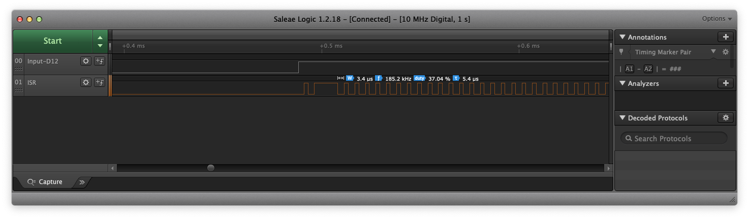
But I noticed something I cannot explain. I instrumented the ISR ( TC3_Handler() ) by having it toggle a pin when invoked. I see that the ISR is being invoked continuously when the input (the waveform) pin is high. After the wave's rising edge, the ISR fires and I see the time taken to sync-read the counter to complete the previous cycle. It returns, but then runs again in 3us - as fast as it can, but there is nothing to do. MC1/MC0 are not set in INTFLAG.

Once the input waveform falling edge arrives, the ISR is not called again until the next rising edge. So I cannot figure out why the handler is being triggered during the pulse phase (high level) of the input.

I added more instrumentation and I see that TC3 INTENA is only what I expect, MC1/MC0. When the ISR is entered over and over, INTFLAG is nothing but SYNCRDY. But that interrupt is not ENAbled, and I even added a write to to INTCLR to make sure it was masked.

Being new to this level of Arduino coding (I've always used it only at the high level before), there's a lot BSP/HAL under here that I have yet to learn. Can anyone shed light? In my case, this could consume 30-40% of the CPU and affect power savings - so, I'm curious :slight_smile:

Images attached, and code below.

Thank you for your time.
-wt

// Setup TC3 to capture pulse-width and period
volatile boolean periodComplete;
volatile uint16_t isrPeriod;
volatile uint16_t isrPulsewidth;
uint16_t period;
uint16_t pulsewidth;

const int     scopePin = 13;

void TC3_Handler(void);

void setup()
{
  Serial.begin(115200);                  // Send data back on the Zero's programming port
  while (! Serial);                      // Wait for the Serial port to be ready

  pinMode(scopePin, OUTPUT);
  digitalWrite(scopePin, LOW);

  REG_PM_APBCMASK |= PM_APBCMASK_EVSYS;     // Switch on the event system peripheral

  REG_GCLK_GENDIV = GCLK_GENDIV_DIV(75) |   // Divide the 48MHz system clock by 75 = 640,000Hz
                    GCLK_GENDIV_ID(5);      // Set division on Generic Clock Generator (GCLK) 5
  while (GCLK->STATUS.bit.SYNCBUSY);        // Wait for synchronization

  REG_GCLK_GENCTRL = GCLK_GENCTRL_IDC |           // Set the duty cycle to 50/50 HIGH/LOW
                     GCLK_GENCTRL_GENEN |         // Enable GCLK 5
                     GCLK_GENCTRL_SRC_DFLL48M |   // Set the clock source to 48MHz
                     GCLK_GENCTRL_ID(5);          // Set clock source on GCLK 5
  while (GCLK->STATUS.bit.SYNCBUSY);              // Wait for synchronization

  REG_GCLK_CLKCTRL = GCLK_CLKCTRL_CLKEN |         // Enable the generic clock...
                     GCLK_CLKCTRL_GEN_GCLK5 |     // ....on GCLK5
                     GCLK_CLKCTRL_ID_TCC2_TC3;    // Feed the GCLK5 to TCC2 and TC3
  while (GCLK->STATUS.bit.SYNCBUSY);              // Wait for synchronization

  REG_EIC_EVCTRL |= EIC_EVCTRL_EXTINTEO3;                                 // Enable event output on external interrupt 3
  //EIC->CONFIG[0].reg |= EIC_CONFIG_SENSE3_BOTH;                           // Set event detecting changes to level

  attachInterrupt(12, TC3_Handler, HIGH);                                 // Attach interrupts to digital pin 12 (external interrupt 3)

  REG_EVSYS_USER = EVSYS_USER_CHANNEL(1) |                                // Attach the event user (receiver) to channel 0 (n + 1)
                   EVSYS_USER_USER(EVSYS_ID_USER_TC3_EVU);                // Set the event user (receiver) as timer TC3

  REG_EVSYS_CHANNEL = EVSYS_CHANNEL_EDGSEL_NO_EVT_OUTPUT |                // No event edge detection
                      EVSYS_CHANNEL_PATH_ASYNCHRONOUS |                   // Set event path as asynchronous
                      EVSYS_CHANNEL_EVGEN(EVSYS_ID_GEN_EIC_EXTINT_3) |    // Set event generator (sender) as external interrupt 3
                      EVSYS_CHANNEL_CHANNEL(0);                           // Attach the generator (sender) to channel 0

  REG_TC3_EVCTRL |= TC_EVCTRL_TCEI |              // Enable the TC event input
                    /*TC_EVCTRL_TCINV |*/         // Invert the event input
                    TC_EVCTRL_EVACT_PPW;          // Set up the timer for capture: CC1 period, CC0 pulsewidth

  REG_TC3_READREQ = TC_READREQ_RREQ |             // Enable a read request
                    TC_READREQ_ADDR(0x06);        // Offset of the CTRLC register
  while (TC3->COUNT16.STATUS.bit.SYNCBUSY);       // Wait for (read) synchronization
  REG_TC3_CTRLC |= TC_CTRLC_CPTEN1 |              // Enable capture on CC1
                   TC_CTRLC_CPTEN0;               // Enable capture on CC0
  while (TC3->COUNT16.STATUS.bit.SYNCBUSY);       // Wait for (write) synchronization

  //NVIC_DisableIRQ(TC3_IRQn);
  //NVIC_ClearPendingIRQ(TC3_IRQn);
  NVIC_SetPriority(TC3_IRQn, 0);      // Set the Nested Vector Interrupt Controller (NVIC) priority for TC3 to 0 (highest)
  NVIC_EnableIRQ(TC3_IRQn);           // Connect the TC3 timer to the Nested Vector Interrupt Controller (NVIC)

  REG_TC3_INTENSET = TC_INTENSET_MC1 |            // Enable compare channel 1 (CC1) interrupts
                     TC_INTENSET_MC0;             // Enable compare channel 0 (CC0) interrupts
  REG_TC3_INTENCLR = TC_INTENCLR_SYNCRDY;

  REG_TC3_CTRLA |= TC_CTRLA_PRESCALER_DIV64 |     // Set prescaler to 64, 640kHz/64 = 10kHz
                   TC_CTRLA_ENABLE;               // Enable TC3
  while (TC3->COUNT16.STATUS.bit.SYNCBUSY);       // Wait for synchronization
}


void loop()
{
  if (periodComplete)                             // Check if the period is complete
  {
    noInterrupts();                               // Read the new period and pulse-width
    period = isrPeriod;
    pulsewidth = isrPulsewidth;
    periodComplete = false;                       // Start a new period
    interrupts();

    Serial.print(period);                         // Output the results
    Serial.print(F("   "));
    Serial.println(pulsewidth);
  }
}


void TC3_Handler()                                // Interrupt Service Routine (ISR) for timer TC3
{
  digitalWrite(scopePin, HIGH);

  // Check for match counter 0 (MC0) interrupt
  if (TC3->COUNT16.INTFLAG.bit.MC0)
  {
    REG_TC3_READREQ = TC_READREQ_RREQ |           // Enable a read request
                      TC_READREQ_ADDR(0x18);      // Offset address of the CC0 register
    while (TC3->COUNT16.STATUS.bit.SYNCBUSY);     // Wait for (read) synchronization
    isrPeriod = REG_TC3_COUNT16_CC0;              // Copy the period
    periodComplete = true;                        // Indicate that the period is complete
  }

  // Check for match counter 1 (MC1) interrupt
  if (TC3->COUNT16.INTFLAG.bit.MC1)
  {
    REG_TC3_READREQ = TC_READREQ_RREQ |           // Enable a read request
                      TC_READREQ_ADDR(0x1A);      // Offset address of the CC1 register
    while (TC3->COUNT16.STATUS.bit.SYNCBUSY);     // Wait for (read) synchronization
    isrPulsewidth = REG_TC3_COUNT16_CC1;          // Copy the pulse-width
  }

  digitalWrite(scopePin, LOW);
}

Sometimes... posing the question, thinking about what to say and what evidence to provide, gets my mind out of a rut and let me find the real problem.

I am attaching the interrupt for pin 12 to the handler. Well, of course; that is the answer. The register reads in the handler do clear the TC3 INTFLAG bits, but do nothing about pin 12's level interrupt.

I've basically set the handler up wrong; what I have in my code is "poll TC3_HANDLER in interrupt context as long as D12 is high".

Sorry to waste all your bandwidth, friends. But thank you for letting me work this out one way or another.

Hi wtsf,

Glad to hear that you've solved the issue.

Just thought I'd mention one further point, as the code example was from one of my earlier attempts at trying to get timer capture working.

Nowadays, I replace the attachInterrupt() function with register calls, because attachInterrupt() still triggers the External Interrupt Controller's (EIC) handler function each time the microcontroller's input pin receives a pulse. This can significantly reduce performance for higher frequency signals. Disabling the interrupts allows the EIC (and event system) to simply act as a conduit through which the external signal is routed to the timer.

This just involves replacing the line (for D12 or port pin PA19):

attachInterrupt(12, NULL, HIGH);

with the code:

EIC->EVCTRL.reg |= EIC_EVCTRL_EXTINTEO3;          // Enable event output on external interrupt 3
EIC->CONFIG[0].reg |= EIC_CONFIG_SENSE3_HIGH;     // Set event detecting a HIGH level
EIC->INTENCLR.reg = EIC_INTENCLR_EXTINT3;         // Disable interrupts on external interrupt 3
EIC->CTRL.bit.ENABLE = 1;                         // Enable EIC peripheral
while (EIC->STATUS.bit.SYNCBUSY);                 // Wait for synchronization

Note the register call to disable the interrupts, allowing the EIC to be used to route the input signal to the timer via the SAMD21's event system without calling the EIC handler function.

Oh, I have not solved my problem :confused:

The reason I changed the 'attachInterrupt' call to name TC3_Handler() instead of passing NULL was because at first, I got no output at all. TC3_Handler() never ran. I was unaware of the weak symbol default handlers underneath the Arduino support, so I tried that change. (Foolish idea for reasons that dawned on me later, as explained above.)

I still cannot get the TC3 interrupts to happen. AFAICT the events are not affecting TC3. My suspicions lie around the NVIC settings for EXINTE03 (for reasons too long to include here).But no; I do not know where the chain of events breaks down.

The interesting observation from my foolish edit is that, somehow, that caused CC0/CC1 to have the right values. Without it, I see them stay zeroed. So providing the Arduino API an explicit handler for EXTINTE03 affected the outcome.

Obviously others had no problems getting this code example to work out-of-the-box. So, I'll keep trying to figure out what's up with my experiment.

Hi wtsf,

It should be possible to get this working.

I noticed that your clocking the timer at 10kHz. Might I ask what frequency and duty-cycle you're using as the input from the 555?

The 555 is on a pot and variable; I'm testing with 70% duty cycle, high about 560ms, low about 240ms. Sorry to be imprecise; I'm away from the test stand right now and haven't been printing out my logs. But that's near what I expect on pin 12 'in real life'. In 'real life; the pulse duty cycles will vary in the range 20%-80% and the periods will be around one second.

Peak-to-peak was, my bad, nearly 5V because the 555 is antique (what I had here on hand to build a test with) and needs 5V. I put a 1Kohm/2.2Kohm divider in 'front' of D12 to limit the input to 3.4V and below. (The real input will be driven at 3.3V.) I double-checked the input pin to be sure I had not damaged the input gate; it's still fine.

I like 10kHz because I can express millisecond intervals clearly in code simply by multiplying them by 10 at compile time, avoiding divides in code at run-time (in other words just do all the timebase math of TC data in a 10x frame of reference); also because 10kHz provides adequate oversampling for 1ms resolution; also because 10kHz is a perfect divider/scaler factor (GCLK 75 , TC 64); also because @10kHz the TC OVF will be set in only a few seconds which will give me timely-enough fault detection of bad inputs (say, if the source has gone offline, cable severed, etc).

I was debugging by printing each component's registers at the start and end of setup() to see if anything was obviously wrong. And what I saw made me doubt my debug code more than help me. The EIC registers do not read back correctly after setup. CTRL.ENABLE was as expected, and CONFIG0 too, but everything else read back as zero. From my reading of the SAMD21 manual, these registers are R/W, do not require synchronization, and should read back correctly (are not read-as-zero/RAZ). I was going to review (again) the EIC registers to be sure. I don't have my logs with me or I would cut/paste them here.