Hey
Whether or not anyone is interested in this, I am not sure, but just something I put together as a test more than anything, and to practice my PCB designing skills again. Its been a while.
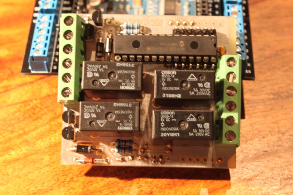
I wanted to make a shield that featured a few small relays so I could switch larger devices, as I couldnt find anyone else who had really done this (no doubt there is however).
I then thought about making a shield with a MCP23S17 SPI IO Expander, as I brought 5 of this a while ago but hadnt played with them yet. I was using Bascom-AVR at that stage and hadnt purchased my first Arduino.
Anyway, I then though - instead of taking up IO from the Arduino to drive these relays, why dont I do this with some of the outputs from the SPI expander.
So what I have made is a prototype PCB with a MCP23S17 chip, of which 4 of the outputs drive 4 BC337 transistors, which in turn drive the coils of 4 5volt relays, which are capable of switching 5 Amps at 230VAC.
The rest of the IO pins I have just made available on header pins, which could be used for anything.
As I say, this is a prototype, and I didnt have enough 0.1" header pins to fully populate the board, but all the functional pins are connected. The others would just be pass through, however the relays are quite tall and so this board would most likely need to be the top most board if stacking anyway.
Designed in Protel DXP 2004 and printed by a company here in NZ who prints single and double sided boards however doesnt have the technology to do via's etc, so these are all done manually. Cheap service though and much better than etching my own boards. And since its a prototype I didnt bother getting them to cut the board out completely, but as you will see it is designed with the proper contours that other arduino shields have.
If/When I make a proper version, it will all be reshuffled as some components arent in ideal places - but its a prototype. Not much room on a shield footprint when using through hole components and relays!
Here are a few snaps incase anyone is interested, sorry the lighting in this room is dim at best and the flash is a bit bright.


This is the test code I used if anyone is interested.
/*Code modified from code I found on http://spikenzielabs.com/SpikenzieLabs/Project_64.html
  Purely to test if the hardware works, which it does.
  Code turns on and off each relay each second
*/

#define            MCP23S17      B01001100      // MCP23017 SPI Address

#define            IOCON            0x0A            // MCP23017 Config Reg.

#define            IODIRA            0x00            // MCP23017 address of I/O direction
#define            IODIRB            0x01            // MCP23017 1=input

#define            IPOLA            0x02            // MCP23017 address of I/O Polarity
#define            IPOLB            0x03            // MCP23017 1= Inverted

#define            GPIOA            0x12            // MCP23017 address of GP Value
#define            GPIOB            0x13            // MCP23017 address of GP Value

#define            GPINTENA      0x04            // MCP23017 IOC Enable
#define            GPINTENB      0x05            // MCP23017 IOC Enable

#define            INTCONA            0x08            // MCP23017 Interrupt Cont
#define            INTCONB            0x09            // MCP23017 1= compair to DEFVAL(A or B) 0= change

#define            DEFVALA            0x06            // MCP23017 IOC Default value
#define            DEFVALB            0x07            // MCP23017 if INTCONA set then INT. if diff.

#define            GPPUA            0x0C            // MCP23017 Weak Pull-Ups
#define            GPPUB            0x0D            // MCP23017 1= Pulled HIgh via internal 100k

#define            OLATA            0x14
#define            OLATB            0x15

#define            INTFA            0x0E
#define            INTFB            0x0F

#define            INTCAPA         0x10
#define            INTCAPB            0x11

// SPI
#define         SS              4                // Pin mapping to Arduino = SELECT
#define         MOSI            6                // Pin mapping to Arduino = Master Out Slave In
#define         SCLK            7                // Pin mapping to Arduino = Serial clock
#define         MISO            5                // Pin mapping to Arduino = Master IN slave OUT

int rx_data = 0;
int buttonPress    = 0;
int error_flag = 0;
int COLUMN = 0;

void setup()
{
  Serial.begin(9600);

  pinMode(SS, OUTPUT);
  pinMode(MOSI, OUTPUT);
  pinMode(SCLK, OUTPUT);
  pinMode(MISO, INPUT);

  digitalWrite(SS, HIGH);
  digitalWrite(SCLK, LOW);
  digitalWrite(MOSI, LOW);

  delay(1000);                               // This delay seems important for the MCP23S17 power-up
  SPI_portexpanderinit();
}

void loop()
{
  //Turns on and off each relay in turn

  SPI_TX(MCP23S17, GPIOA, B00000000);
  SPI_TX(MCP23S17, GPIOB, B00000000);
  delay(1000);
  SPI_TX(MCP23S17, GPIOA, B00000001);
  delay(1000);
  SPI_TX(MCP23S17, GPIOA, B00000000);
  delay(1000);
  SPI_TX(MCP23S17, GPIOA, B00000010);
  delay(1000);
  SPI_TX(MCP23S17, GPIOA, B00000000);
  delay(1000);
  SPI_TX(MCP23S17, GPIOB, B10000000);
  delay(1000);
  SPI_TX(MCP23S17, GPIOB, B00000000);
  delay(1000);
  SPI_TX(MCP23S17, GPIOB, B01000000);
  delay(1000);
}

void SPI_portexpanderinit()
{
  // --- Set I/O Direction
  SPI_TX(MCP23S17,IODIRB,B00000000);                                 // MCP23S17 port B = OUTPUT
  SPI_TX(MCP23S17,IODIRA,B00000000);                                 // MCP23S17 port A = OUTPUT

  //  --- Clear ALL Bits of GPIOA and GPIOB
  SPI_TX(MCP23S17,GPIOB,B00000000);                                  // MCP23S17 Clear port B
  SPI_TX(MCP23S17,GPIOA,B00000000);                                  // MCP23S17 Clear port A

}

void SPI_TX(int device, int regadd, int tx_data)
{
  digitalWrite(SS, LOW);                                       // Select the Chip

  device = device & B11111110;                                 // Clear last bit for a write

  SPI8BITTXLOOP(device);                                       // SPI Device

  SPI8BITTXLOOP(regadd);                                       // SPI REGISTER ADDRESS

  SPI8BITTXLOOP(tx_data);                                      // Data

  digitalWrite(SS, HIGH);                                      // Done UN-Select the Chip
}

void SPI8BITTXLOOP(int data)
{
  int i = 0;
  int temp = 0;

  for(i=1; i < 9; i = i +1)
  {
    temp = (data >> 7);                                        // Test bit 7 of DATA
    temp = temp & 1;
    if (temp == 0)                                             // SET or CLEAR MOSI
    {
      digitalWrite(MOSI, LOW);
    }
    else
    {
      digitalWrite(MOSI, HIGH);
    }
    digitalWrite(SCLK, HIGH);                                   // SET SCLK
    digitalWrite(SCLK, LOW);                                    // Clear Clock
    data = data << 1;                                           // Shift data LEFT by 1
  }
}