Building a working flash memory programmer.

I am working on making a z80 based CPM computer based on the design from Grant Searle - http://searle.hostei.com/grant/ - and have been studying up what would be needed to make a go of it. With the passage of time some electronic devices have gotten more expensive, and some have gotten cheaper. For a ROM, the current cheapest way that I could find for a 1-off board is one of the 128Kx8bit memories. An SST39SF010A is only $1.66US at Digikey, and a 628128 128Kx8bit RAM is $2.15US.

NOTE: This programmer will never be a standalone device. A goal is that I could send it a IntelHex file and it would read each line and write it to the flash, with the PC based program checking for addresses used, and offsets I might want to put on the data (more than 1 ROM image on a chip for testing/playing) In this case the Erase and write and verify could be automated. The other possibility is that I would send data to it in a binary mode which would be dependant on a program in another computer to send it address and data.

The biggest problem is this - How do I program one of these Flash ROMS? And it turns out it is really rather easy. I started out with a design that uses an Arduino and 3 74595 shift registers, and then I dug out a board that I had put together a while back - ATMega1284P-PU 40 pin DIP based board that Crossroads pproduced and I bought a bare board form him. Here's the where the conversation can be found - ATmega1284P: End to End using 1.0 IDE - Microcontrollers - Arduino Forum. I hadn't done much with the board for awhile and recently I purchased several USB to Serial converters form DIPMicro and got one of them wired up and working.

So I went from trying to design it with an ATMega328P and 3 supporting 595 shift registers to needing 1 ATMega1284 and no supporting chips.. The ATMega1284 is a 40 pin DIP device with 32 I/O pins, of which can use up to 2 serial ports. In this application I only need 1 serial port so 30 pins are left free. The 8 pins for PORTA are assigned to the Flash's 8 data pind, PORTC is the lower 8 address bits, and because of the way things are defined under the Bobuino the other pins move around so they are not as easy to map to a port. So 2 Serial Port Pins, 8 Data bits, 19 address bits and 3 control bits - (*OE, *WE,*CE) and all the pins are used.

and because of the way things are defined under the Bobuino the other pins move around so they are not as easy to map to a port.

I don't quite follow that.
The Serial pins are in the middle of Port D - Atmel's call on that.
Using Port A for 8-bit data,
Port C for address byte, Port B for address byte,
one pin of Port D for 17th18-19 address bit,
other pins of Port D for control lines.

Then direct port manipulation to set things up, so something along these lines:

PORTA = dataByte[19bitAddress]; // data to be written from an array
PORTB = lowAddress;
PORTC = highAddress;
// manipulate PORTD appropriately for 3 address bits, such as:
PORTD = PORTD & 0b11100011; // clear 17th-18-19 address bit, or
PORTD = PORTD | 0b00011100; // set 17th-18-19 address bit - Bit 2,3,4 for example

PORTD = PORTD & 0b10011111; / clear CE Bit 5, WE bit 6
PORTD = PORTD | 0b01100000; // set CE, WE
PORTD = PORTD & 0b01011111; // clear CE Bit 5, OE Bit 7
dataRead = PINA; // read the device's data
PORTD = PORTD | 0b10100000; // set CE, OE
if (dataRead == dataByte[19bitAddress]){
// go on to next address
lowAddress = lowAddress +1;
if (lowAddress ==0){
highAddress = highAddres +1;
if (highAddress == 0){
PORTD = PORTD | 0b00000100; // set address bit 17
:
:
similar for other other address bits
}
}
}
19bitAddress =( (PORTD & 0b00011100) <<14) | (highAddress <<8) | lowAddress; // 14 correct? confirm
}

}

I think you can see the idea tho.

Totally independent of what Bobuino might name the pins, and fast too.

I have previously worked with Direct Port Manipulation on a Stepper Driver I made using an ATtiny2313 so I wanted to use that here wherever possible. Direct Port I/O is faster, but on a standard Arduino the use is limited by other functions sharing the different ports and the ATMega328. On the 1284 configured like a Bobuino, PORTA - which is shared with the 8 Analog pins (A0-A7) and (D14-D21) and PORTC which is digital pins D22-D29.

I assigned the Flash Data pins to PORTA and the lower 8 address bits to Port C.

I can read the chip ID, and I can read chip data.

Reading the chip data is the easiest. Load an address onto the address lines,

digitalWrite(ReadEN,LOW);
digitalWrite(ChipEN,LOW);
readVal = PINA;
digitalWrite(ChipEN,HIGH);
digitalWrite(ReadEN,HIGH);

I am working on using the "sector" operations. Sectors are 4K blocks of memory. So a sector runs from address XX000 to XXFFFF. So to read secto 0 the command is R00, to read sector stating at 7000 the command would be R07. It will read a 4K sector and send it out the serial port in approx. 10 seconds.

The CHip ID function uses both Write and Read. It writes to a sequence of addresses and then any address ending in 0 will return the Manufactirer ID, and any address ending in 1 will return the Chip ID. The sequence for the Chip ID function is -
Write to address 5555 the value AA,
write to address 2aaa the value 55,
Write to address 5555 the value 90,
then read from and Even address the Chip Manufacturer ID,
and from and Odd address the Chip ID.
and when finished send 0f to any address to exit Chip ID Mode.

These 2 functions are Non-Destructive, but when the Chip-ID function works properly then all programming steps should also work.

Hey Crossroads - Here's where I come up with that -

On the Bobuino PORTB goes like this - Pin 1 D4, Pin2 d5, pin3 D6, Pin4 D10, Pin5 D11, Pin6 D12, Pin7 D13
and on PORTD Pin1 RX0, Pin2 TX0, Pin3 D2, Pin3 D3, Pin4 D30, Pin 5 D8, Pin6 D9, Pin7 D31.

As is, I got a few wires mixed up and I was just going from PinX on the Crossroads Bobuino board to PinY on the flash chip. By not trying to sort out the pins at this time I felt I had a higher degree of possibility of not getting myself confused and haveing it work, WHICH IT NOW DOES!!! I have successfully WRITTEN, READ and Erased a Sector of the flash. 90% finished. Took about a week. Now the remaining 10% will take months...

If I used just PORT I/O it would work, but there would be 2 levels of numbers to keep track of the get all the wires in the proper place. If I used a "Standard" pin configuration then the individual PORT groups would not be mixed up in any manner.

Just a matter of the number of things I want to juggle when I am not real sure what I am doing.
As is, I got a few wires mixed up and I was just going from PinX on the Crossroads Bobuino board to PinY on the flash chip. By not trying to sort out the pins at this time I felt I had a higher degree of possibility of not getting myself confused and having it work, WHICH IT NOW DOES!!! I have successfully WRITTEN, READ and ERASED A SECTOR of the flash. 90% finished. Took about a week. Now the remaining 10% will take months...

If I make another Flash Programmer ) will get a 1284 and a couple caps, a resistor, a switch and a resonator and make a 1 chip, 1 socket programmer using the "Standard" configuration.

I have attached a drawing I made comparing the pinouts, Bobuino to Standard.

1284s.bmp (2.58 MB)

Here's what I have programmed so far -

I'll Start with the configuration information.
This is programmed around an ATMega1284P-PU 40 Pin DIP Device. A total of 32 I/O lines with 2 of them used as Serial 0, leaving 30 free I/O lines.

To the Arduino 1.0.5 environment I added the mighty-1284p hardware information and I am using the Bobuino board configuration.

When referring to the Address or Data busses I am referencing the socket for the SST39SF type Flash Memory.

The Data Buss uses PORTA on the 1284 which corresponds to Pins D14 through D21 on the.Bobuino. (also serve as analog pins)

the lower 8 bits of the Address buss correspond to PORTC which is pins D22 through D29.

The three remaining pins are the 3 enable pins. On this type of memory device the are an ACTIVE LOW signal, meaning that the signal is active when at zero volts and inactive at 5 volts. ReadEN and WriteEN both work with ChipEN to control the memory.

// Address bits -
// bits 0-7 are PORTC
// Because this board is using BOBUINO pinouts
// 
int AB8 = 2; 
int AB9 = 3; 
int AB10 = 4; 
int AB11 = 5; 
int AB12 = 6; 
int AB13 = 7; 
int AB14 = 8; 
int AB15 = 9; 
int AB16 = 10; 
int AB17 = 11; 
int AB18 = 12; 


int ChipEN = 13;
int ReadEN = 30;
int WriteEN = 31;

The Setup Function -

Setup configures the various pins to communicate with the Flash chip. The Control Lines and Address Lines are always writing to the flash so they are easy to configure as outputs, along with configuring the Serial port.

Controls Lines are set to 5 volts and all the address lines are set to 0zero volts to begin.

void setup()
{
   Serial.begin(115200);
   
   // set control signals to HIGH
   pinMode(ChipEN,OUTPUT);
   digitalWrite(ChipEN,HIGH);
   pinMode(ReadEN,OUTPUT);
   digitalWrite(ReadEN,HIGH);
   pinMode(WriteEN,OUTPUT);
   digitalWrite(WriteEN,HIGH);
   
   // configure the address lines
   DDRC = 255;
   PORTC = 0;
   pinMode(AB8,OUTPUT);
   digitalWrite(AB8,0);
   pinMode(AB9,OUTPUT);
   digitalWrite(AB9,0);
   pinMode(AB10,OUTPUT);
   digitalWrite(AB10,0);
   pinMode(AB11,OUTPUT);
   digitalWrite(AB11,0);
   pinMode(AB12,OUTPUT);
   digitalWrite(AB12,0);
   pinMode(AB13,OUTPUT);
   digitalWrite(AB13,0);
   pinMode(AB14,OUTPUT);
   digitalWrite(AB14,0);
   pinMode(AB15,OUTPUT);
   digitalWrite(AB15,0);
   pinMode(AB16,OUTPUT);
   digitalWrite(AB16,0);
   pinMode(AB17,OUTPUT);
   digitalWrite(AB17,0);
   pinMode(AB18,OUTPUT);
   digitalWrite(AB18,0);
  
}

Now for the start of the general purpose routines.

To start with - LoadAddr.

This function takes an unsigned long value and uses it to set the Address Lines for any read or Write function.
This function would need to be re-arranged if I wer to use a standalone 1284 and use the Mighty 1284 board rather than the Bobuino.

Because the lowest 8 address bits are all assigned to PORTC I just copy the lowest 8 bits to that port and then use shifts to move the rest of the bits into the address lines.

void LoadAddr(unsigned long AddressL)
{
   unsigned long workAddrL;
   workAddrL = AddressL;
   PORTC = workAddrL & 0xFF;
   workAddrL= workAddrL >> 8;
   digitalWrite(AB8, workAddrL & 1);
   workAddrL= workAddrL >> 1;
   digitalWrite(AB9, workAddrL & 1);
   workAddrL= workAddrL >> 1;
   digitalWrite(AB10, workAddrL & 1);
   workAddrL= workAddrL >> 1;
   digitalWrite(AB11, workAddrL & 1);
   workAddrL= workAddrL >> 1;
   digitalWrite(AB12, workAddrL & 1);
   workAddrL= workAddrL >> 1;
   digitalWrite(AB13, workAddrL & 1);
   workAddrL= workAddrL >> 1;
   digitalWrite(AB14, workAddrL & 1);
   workAddrL= workAddrL >> 1;
   digitalWrite(AB15, workAddrL & 1);
   workAddrL= workAddrL >> 1;
   digitalWrite(AB16, workAddrL & 1);
   workAddrL= workAddrL >> 1;
   digitalWrite(AB17, workAddrL & 1);
   workAddrL= workAddrL >> 1;
   digitalWrite(AB18, workAddrL & 1);
}

DoRead takes an address as an unsigned long and passes it to LoadAddr() to load the Address Lines and then sets ReadEN and ChipEN LOW and then using the PINA instruction reads the value present on the Data Lines. The it sets ChipEN and ReadEN High and returns the value read.

DDRA = 0 sets PORTA as an input. PORTA = 0 makes sure

byte DoRead(unsigned long readAddr)
{
   byte readVal; 
   LoadAddr(readAddr);
   DDRA = 0;    // set PORTA as all inputs from Flash Data Lines
   digitalWrite(ReadEN,LOW);
   digitalWrite(ChipEN,LOW);
   readVal = PINA;
   digitalWrite(ChipEN,HIGH);
   digitalWrite(ReadEN,HIGH);
   return readVal; 
}

DoWrite takes both an unsigned long address and a byte to write to the Flash. The address is passed to LoadAddr() and the byte is loaded into PORTA ,ChipEN and WriteEN lines a re set to LOW and then ChipEN and WriteEN are set back to HIGH.

void DoWrite(unsigned long writeAddr, byte writeVal)
{
    LoadAddr(writeAddr);
    DDRA = 255;    // set port A as all outputs to Flash Data Lines
    PORTA = writeVal;
    digitalWrite(ChipEN,LOW);
    digitalWrite(WriteEN,LOW);
    digitalWrite(ChipEN,HIGH);
    digitalWrite(WriteEN,HIGH);
}

These are the common routines that the rest of the program uses to read and write the Flash.

Now for a routine that makes use of these previous routines.

To read the Manufacturers ID and the Device ID requires a sequence of writes and then a 2 reads to collect this information. The sequence is as follows -
At address 0x5555 write 0xAA,
at address 0x2AAA write 0x55,
at address 0x5555 write 0x90,
then do a read from address 0 to obtain the Manufacturer ID,
and a read for address 1 to obtain the Device ID
and then to exit the ID mode write 0xF0 to any address.

From my experience - if you fail to write 0xF0 to close out the Device ID mode future reads may give random results.

void DeviceID()
{
   byte WorkByte;
   Serial.println();
   Serial.println("Device Identification");
   Serial.println();
   DoWrite(0x5555L,0xAA);   // First output byte of Software ID Entry
   DoWrite(0x2AAAL,0x55);   // Second output byte of Software ID Entry
   DoWrite(0x5555L,0x90);   // Third output byte of Software ID Entry
   WorkByte = DoRead(0L);
   if (WorkByte == 0xBF)
   {
      Serial.println("Chip Manufactured by SST");
   }
   else
   {
      Serial.println("Unkmown manufacturer");
   }
   WorkByte = DoRead(1L);
   if (WorkByte == 0xB5)
   {
      Serial.println("SST39SF010");
      Serial.println("128Kx8 Device");
      Serial.println("131,072 Bytes");
   }
   else if (WorkByte == 0xB6)
   {
      Serial.println(" SST39SF020");
      Serial.println("256Kx8 Device");
      Serial.println("262,144 Bytes");
   }
   else if (WorkByte == 0xB7)
   {
      Serial.println(" SST39SF040");
      Serial.println("512Kx8 Device");
      Serial.println("524,288 Bytes");
   }
   else
   {
      Serial.println(" Unknown Device");
   }
   Serial.println();
   DoWrite(0x5555L,0xF0);   // Exit ID Mode
}

Next step - pull in data from serial port to load into the part?

CrossRoads:
Next step - pull in data from serial port to load into the part?

That's right. Now for the routines that do the real work...

I have 3 things I need to do to program the Flash chips. Need to be able to write (Program) the chip, Read (to verify) and Erase.

The Erase can be done in 2 different ways. Whole Device or by "Sector". in this case a sector is defined as a 4K (4096 byte) block of the Flash. I am using the Sector Erase as I am planning on haveing more than 1 ROM image present on the chip so why erase it all when I just want to mess with just 1 - 16K section.

Because I am planning on automating this from a program on the PC feeding the programmer I can easily erase multiple sectors very easily. A sector is addressed using just the upper address lines so on the 39SF010 chips I am using the sectors are addressed from sector 00 to sector 1F. These represent 4K blocks starting at addresses ending with 000, or 00000, 01000,02000, 03000 on to 1F000. to erase multiple sectors all I have to do is send a command string like this - S00S01S02S03 and those four sectors will be reset back to all FF. *The datasheet gives the time to fininsh the operation but it appears that the ASrduino code is slow enough that the erase time is not a problem. A delay could be added to the Sector Erase function if needed/wanted.

Reads and Writes will be done in 16 byte blocks. I could do bigger blocks so this is just my choice. To read 16 bytes the command starts with Rand then has a 5 hex digit addess. The programmer responds with a string of Hec digits - 5 digits for the address, a colon(:), and then the sixteen values -
Command - R08020
Response - 08020:000102030405060708090A0B0C0D0E0F

And for the Write - This command will start with a "W" and then have a 5 hex digit address, a colon(:), and then 16 hex bytes. It looks just like the response for Read but with a W at the start. It wil call the Read function to verify the write.
Command - W08020:000102030405060708090A0B0C0D0E0F
Response - 08020:000102030405060708090A0B0C0D0E0F

Now for several more helper routines -

First one takes a long or unsigned long and pronts out 5 hex digits.
I use only 4 bits at a time because the Serial.print( ,HEX) does not print lading zeros. In other words - printing the value 15 usint the ,HEX option in print will only print F and for an 8 bit value I want 0F printed. So I process each nibble and print out the hex equivelent.

void PrintHex5(unsigned long PrintVal)
{
   Serial.print((PrintVal >> 16) & 0xF,HEX);
   Serial.print((PrintVal >> 12) & 0xF,HEX);
   Serial.print((PrintVal >> 8) & 0xF,HEX);
   Serial.print((PrintVal >> 4) & 0xF,HEX);
   Serial.print(PrintVal & 0xF,HEX);
}

And to go the other way, because I am giving a 5 digit hex address to the Read and Write functions -
5 digit HEX in, and unsigned long out.

unsigned long Asc52Long(char *srcStr)
{
   int ctr;
   int tmpChar;
   unsigned long tmpLong = 0L;
   for (ctr = 0; ctr < 5; ctr++)
   {
       tmpChar = srcStr[ctr];
       tmpChar = tmpChar & 0x4F;
       if (tmpChar > 9) 
       {
          tmpChar = (tmpChar & 0xF) + 9;
       }
       tmpLong = (tmpLong << 4) + tmpChar;
   }
   return tmpLong;   
}

And to convert the individuall byte values that are being given to the Write function.
2 digit hex in, and byte out.

byte Asc22Byte(char *srcStr)
{
   int ctr;
   char tmpChar;
   char workChar = 0;
   for (ctr = 0; ctr < 2 ; ctr++)
   {
       tmpChar = srcStr[ctr];
       tmpChar = tmpChar & 0x4F;
       if (tmpChar > 9) 
       {
          tmpChar = (tmpChar & 0xF) + 9;
       }
       workChar = (workChar << 4) + tmpChar;
   }
   return workChar;
}

Now for the functions that the user interfaces with -

Read from the flash. This function takes an address - 5 digit HEX - from the serial port and then prints out the addres - 5 digit hex - a colon(:slight_smile: and then 16 bytes in hex.
This is the cammansd to read from the flash
R00200 to read from address 0x200 - 0x20F

void ReadFlash()
{
   unsigned long ctr;
   unsigned long ReadAddrL;
   char ReadNiblLo, ReadNiblHi;
   char ctrPrt, readVal;
   
   char strAddress[8]={'\0','\0','\0','\0','\0','\0','\0','\0'};
   do
   {
      Serial.readBytes(strAddress,5);
   }while(strAddress[0]==0);
   ReadAddrL = Asc52Long(strAddress);
   //Serial.print("Starting address = ");
   //PrintHex5(ReadAddrL);
   //Serial.println();
   for (ctr = ReadAddrL; ctr < (ReadAddrL + 0x10); ctr++)
   {
       ctrPrt = lowByte(ctr) & 0xf;
       if (ctrPrt == 0)
       {
          PrintHex5(ctr);
          Serial.print(":");   
       }
       readVal = DoRead(ctr);
       ReadNiblLo = readVal & 0xF;
       ReadNiblHi = (readVal >>4) &0xF;
       Serial.print(ReadNiblHi,HEX);
       Serial.print(ReadNiblLo,HEX);
   } 
   Serial.println();
}

And to Write to the flash you send the programmer a W, followed by 5 hex digits for the start address and 16 bytes in hex.
W00200:C3284915382010A239FF3EAA55012122 will write to addresses 0x200 - 0x20F

Prior to writing the flash, all bytes to be written to must be 0xFF or the results may no be predictable. If necesary the sector (4k block) that you wish to write to must be erased before writing.

To write 1 byte to the flash 4 bytes must be written, The first 3 are to special addresses. The sequence is this -
to address 0x555 write 0xAA, then to address 0x2AAA write 0x55, then to address 0x5555 write 0xA0 (the code to select Program Mode) and then to the desired address write the desired byte. Repeat this sequence for each byte you wish to write.

When the write sequence completes, the 16 bytes just written are read back and sent to the serial port.

void WriteFlash()
{

    unsigned long ctr;
   unsigned long WriteAddrL;
   char ReadNiblLo, ReadNiblHi;
   char  readVal, writeVal, hexVal[3];
   char strAddress[8]={'\0','\0','\0','\0','\0','\0','\0','\0'};
   char chkColon[3] ={'\0','\0','\0'};
   char WriteData[33] = {'\0','\0','\0','\0','\0','\0',
                         '\0','\0','\0','\0','\0','\0',
                         '\0','\0','\0','\0','\0','\0',
                         '\0','\0','\0','\0','\0','\0',
                         '\0','\0','\0','\0','\0','\0',
                         '\0','\0','\0'};
   do
   {
      Serial.readBytes(strAddress,5);
   }while(strAddress[0]==0);
   WriteAddrL = Asc52Long(strAddress);
   //Serial.println(WriteAddrL,HEX);
   do
   {
      Serial.readBytes(chkColon,1);
   }while(chkColon[0]==0);
   do
   {
      Serial.readBytes(WriteData,32);
   }while(WriteData[0]==0);
   for (ctr = 0 ; ctr <  16; ctr++)
   {
      hexVal[0] = WriteData[ctr *2];
      hexVal[1] = WriteData[ctr *2 + 1];
      hexVal[3] = 0;
      writeVal = Asc22Byte(hexVal);
      DoWrite(0x5555L,0xAA);   // First output byte of Byte Program 
      DoWrite(0x2AAAL,0x55);   // Second output byte of Byte Program
      DoWrite(0x5555L,0xA0);   // Third output byte of of Byte Program
      DoWrite(WriteAddrL+ctr,writeVal);   // Address and Data to store
   }
   //Serial.println();
   PrintHex5(WriteAddrL);
   Serial.print(":");   
   for (ctr = 0 ; ctr <  16; ctr++)
   {
      readVal = DoRead(WriteAddrL+ctr);
      ReadNiblLo = readVal & 0xF;
      ReadNiblHi = (readVal >>4) &0xF;
      Serial.print(ReadNiblHi,HEX);
      Serial.print(ReadNiblLo,HEX);
   } 
   Serial.println();


}

And the Sector Erase command. There are 2 erase commands for this device. The Sector Erase and the Device Erase. I have not implemented the Devie Erase as I am sure I would use it at the worst possible time and erase everything and leave myself very frustrated. The Sector Erase will a 4k block of the flash starting from a 4K page boundry. Pages start at an address ending with 3 zeros - 00000, 01000, 08000, 0f000, 1F000 so the command just requires the first 2 digits. To erase the 4 k sector at 0x0e000 the command is S0E
The Sector Erase command writes a sequence of bytes to specific addresses as follows -
to address 0x5555 write 0xAA,
to address 0x2AAA write 0x55,
to address 0x5555L write 0x80,
to address 0x5555L write0xAA,
to address 0x2AAAL write 0x55,
and then to the to the EraseAddress write 0x30

void SectorErase()
{
   unsigned long EraseAddrL;
   char Sector[3]={'\0','\0','\0'};
   do
   {
      Serial.readBytesUntil(13,Sector,2);
   }while(Sector[0]==0);
   Sector[0]= Sector[0] & 0x0F;
   Sector[0]= Sector[0] <<4;
   Sector[1]= Sector[1] - 0x30;
   if (Sector[1] > 0x9)
   {
      Sector[1] = (Sector[1] & 0xF) + 9;
   }
   EraseAddrL = Sector[0] | Sector[1];
   EraseAddrL = EraseAddrL << 12;
   PrintHex5(EraseAddrL);
   Serial.println();
   DoWrite(0x5555L,0xAA);   // First output byte of Sector Erase 
   DoWrite(0x2AAAL,0x55);   // Second output byte of Sector Erase
   DoWrite(0x5555L,0x80);   // Third output byte of Sector Erase
   DoWrite(0x5555L,0xAA);   // Fourth output byte of Sector Erase
   DoWrite(0x2AAAL,0x55);   // Fifth output byte of Sector Erase
   DoWrite(EraseAddrL,0x30);   // Sector Address and 0x30 Sector Erase Command
}
And here's a diagram of how it is currently wired.

1 - ATMega1284P on a Bobuino type Board
1 socket for 1 - SST39SD010/020/040 Flash PROM.

It was wired to match the pin order in the Bobuino board description. Now that I have got it functioning I will rearrange some wires so I can also write address lines 8-15 using PORTB and see if that speeds up the operation a bit.

Numbers in Red are the Pin Names from the device. Numbers in Green are the pin Numbers. Number in Blue are the 1284 pin names from the Bobuino Board.

FlashWiring.bmp (2.58 MB)

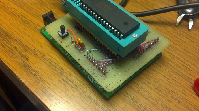
And here are a couple pictures.

Serial interface and ZIF socket from DIPMicro. Bobuino board from CrossRoads. Remainder from the junkbox.

And YES, that is wired using wire-wrap.

And for more wire-wrap - anyone know where I could find some 0.025 inch square brass wire? Wire-wrap sockets are getting expensive and hard to find, but with some 0.025 square wire I could adapt some regular sockets and then wire-wrap away...

Smaller pics -like 1000 wide, 3000+ is too wide.

Sockets are not hard to find - I get them from here, altho usually just strips vs sockets for ultimate flexibility - cost per/pin is the same I think.
http://www.king-cart.com/phoenixent/product=SOCKETS+WIRE+WRAP+DIP+%2526+SIP/exact_match=exact

I don't know about wire.

I got home last friday and for somereason, when I plug my Flash Programmer shield into my Bobuino board there is a voltage problem...

So I started a new board with just the minimal parts to make a programmer. I have a socket for the ATMega1284, a 16MHz resonator, a 10k resistor for a Reset pullup, a NO Pushbutton, an LED and 560 ohm resistor for a power light, a couple caps under the 1284, a socket for the flash and a 5 pin header for the serial adapter. Wired it up using some CT5 nextwork wire and got it working. Had to redo a couple wires, and rework the program slightly.

By re-arranging the i/o slightly I was able to use both PORTC and PORTB for address bits and the end result its that it runs faster. was bout 15 minutes to write, and last night I was seeing a time of 2 Minutes 50 Seconds. Anything that speeeds up the setting of the address lines will have a great impact on write times. To write 1 byte requires 4 different addresses to be written to so the LoadAddr function gets a workout.

Cool. Using direct port manipulation also for the control lines?

Haven't gotten there yet....

Some calulations, the right combination of ands and ors and iI should be able to make it work. The 3 control pins can all be set to HIGH when setting up the address pins so that does simplify the work to set the address lines. then the read and the write functions will do the ands and ors. Hmmm, what's the idle state of the serial pins?

Got sidetracked playing with Eagle and produced a routed board in about 2 hours. And then I got distracted by trying to create some boards for the z80 CPM computer, can't call it a single board computer because of the board size limits fir the free version of Eagle mean I will need to stack a couple boards....

I got the board working using Direct Port Manipulation for all i/o to the SST39sf010 and the results are up in the air.

PORTA - PINA - write and read teh data lines.

PORTC - write address lines A0 - A7
PORTB - write address lines A8-A15

PORTD PD0 & PD1 are serial0, PD2 - A16, PD3 - A17, PD4 - A18, PD5 - ChipEnable, PD6 - OutputEnable, PD7 - WriteEnable.

void LoadAddr(unsigned long AddressL)
{
   unsigned long workAddrL;
   unsigned int PDHold;
   workAddrL = AddressL;
   PORTC = lowByte(workAddrL);
   PORTB = highByte(workAddrL);

   PDHold = PORTD & 0xE3;   // mask out the control bits and the serial port bits.
   PDHold= PDHold  | ((workAddrL >> 14) & 0x1C);  // address bits 16, 17, 18 to PORTD bits 2, 3, 4
   PORTD = PDHold; 

/*   
   workAddrL= workAddrL >> 16;
   digitalWrite(AB16, workAddrL & 1);
   workAddrL= workAddrL >> 1;
   digitalWrite(AB17, workAddrL & 1);
   workAddrL= workAddrL >> 1;
   digitalWrite(AB18, workAddrL & 1);
*/  

}

I need to compare the highByte() and lowByte() functions to this -
PORTC = workAddrL & 0xFF;
workAddrL = workAddrL >> 8;
PORTB = workAddrL & 0xFF;
workAddrL = WorkAddrL >> 6; // shift 6 because the 2 lowest bits of PORTD are the serial port
workAddrL = workAddrL & 0x1C; // just bits 3, 4, 5
PORTD = workAddrL | 0xE0; // top 3 bits need to be HIGH , are active LOW and I am just setting the address bits here.

I had to add 2 delays to give the control signals time to stabilize and have time to read or write the data to/from the device and I didn't gain any significant speedup over using digitalWrite s to set the top 3 address bits and 2 of the 3 enable pins. I am doing 32bit math, so the next thing would be to see if I could do 16 bit math and see if that would speed anything up, or if the extra code would just slow things down someplace else.

Seems like the hard way to do things.
Just keep track of the address in 3 chunks. lower 8, next 8, upper whatever is left.
increment each individually, when one rolls over increment the next one.

lower8 = lower8 +1;
if (lower8 == 0){
upper8 = upper8 +1;
if (upper8 == 0){
highBits = highBits +1;
// and reset highBits to 0s when you start a new write sequence.
}
}
}
then
PORTB = lower8;
PORTC = upper8;
PORTD = PORTD & 0b11111000; // clear out the 3 bits
PORTD = PORTD | (highBits);

that's got to be a lot faster than 32 bit math and all that shifting.

One step at a time. Make it function, and then change one thing at a time and keep it functioning.