After I have implemented a VGA interface on TinyFPGA-BX, 640x480@60Hz, 25 MHz pixel clock,
where it works very nice, I've included it into VIDOR4k.
No hope to have a perfect display, there is a jittering pixel positions.
Well, observed at oscilloscope the HSYNC edge on TinyFPGA-BX is perfectly stable
observing it at 350 us after the trigger (after about display 11 lines from the triggering one).
But on VIDOR4k this jitter is +/- 125 ns which correspond to 125/20 = about +/6 pixels.
Horizontal sync random jitter --> horizontal jittering position because both HSYNC and RGB
timing have the same jitter.
What to do?
I've generated a second PLL for the VGA, trying with slow loop filter and no compensation mode,
both reported as methods to reduce the jitter, but nothing is changed.
I've nuffered the HSYNC and VSYNC outputs to reduce the output current, no changes.
Someone has implemented a VGA on VIDOR4k?
Results?
Hints?
Both clocks iCLK, 48 MHz coming from processor, and internal one wOSC_CLK coming from
cyclone10lp_oscillator instance, about 66 MHz, have high jittering.
As soon as possible I'll cut the iCLK CPU-FPGA interconnection and I'll insert a
stable 48 MHz oscillator.
I've found R28 on the pcb, cut the track from the processor, inserted a MEMS
oscillator CMOS 3.3V.
Powered the board the oscillator starts, I can see it, 48 MHz, but the
high level seem unstable, sometimes but repetively drops down to about 2.5 V.
Looking at VCC on the board pin I can see why:
each 70 ms the is a drop from 3.3V down to about 2.5V, it seems there is something
drawing an extra current, doesn't matter is I press the reset button.
The +5V are stable.
So it seems related to my clock always running, not to oscillator itself
that consumes some mA.
Questions:
is the attached schematic true so if I cut the connection cpu-R28 the GCLK doesn't drive anything?
I know the GCLK is started at a given point from the CPU program: if it is always active like
with my oscillator, what kind of problems can arise?
Is the FPGA that begins to read the configuration memory and makes some bus contention?
Alternative: put the oscillator on the iMIPI_CLK LVDS input on camera connector.
I've tried in all ways, the iMIPI_CLK(n) set at VCC/2 and 1.1V, iMIPI_CLK directly driven by the
oscillator.
I can see a perfect 48 MHz clock, the iMIPI_CLK/iMIPI_CLK(n) differential clock has a 3.3V swing
centered at 1.6 or 1.1V, but I can't see it internally to the FPGA.
Maybe the swing and/or the common mode bias point are wrong?
Limba:
Can you meas VSYS and VCRG it shouldn't drop under 3v3.
Edit:Are you using USB or external PSU for VIN
Power from USB.
With my oscillator the +5V on the board pin is quiet,
3v3 behaves as described.
The GCLK feeds FPGA E2 pin only.
What happens if this clock is active at power-up instead after the power-up
when the software starts it?
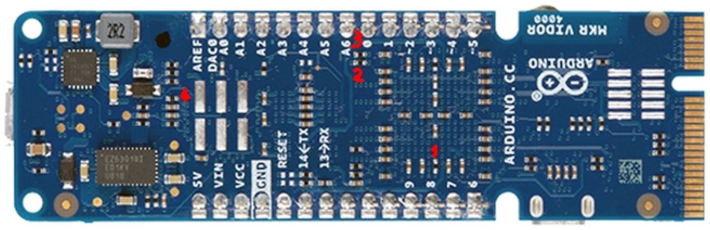
On the FPGA there is my own project, the only FPGA pins I use are
Ax and Dx that appear on the two standard male/female board connectors.
Yes, I could mount a manual switch to insert my oscillator after
the complete board startup, but ... no one of the board hardware
and software designers is able to explain why the GCLK is started in the following way?
I need to check that 3v3 from my vidor. Currently using zedboard for tinkering.
Is that dropping 3v3 seen only when using external crystal?
What I see is charging chip that needs to be configured by SW to get right charging and USB current limit. Not sure will arduino do this at startup.
One way is to use Lion battery for that J12 connection. That will bypass current limit made by USB power/charging controller
Edit:
If that charging chip detect normal USB then it sets 100mA as specs requires and SW need to update current limit after it negotiate host for bigger current limit.
If it detects USB charger then it's uses limits set by charger.
Determination for normal connection to USB is that D+ and D- is floating after 0.5s after startup. After that SW can go and increase USB current.
Limba:
I need to check that 3v3 from my vidor. Currently using zedboard for tinkering.
Is that dropping 3v3 seen only when using external crystal?
Yes, seen ONLY with my external oscillator powered AND connected to R28 side CPU,
with connection R28-CPU prevoiusly interrupted (track cut)
My oscillator is a DSC6021JE3B-01GB sample from Microchip, it draws 1.3 mA only.
With my oscillator always powered, if I detach its output and restore the connection R28 to CPU
the boards return to work again (3v3 stable).
Limba:
What I see is charging chip that needs to be configured by SW to get right charging and USB current limit. Not sure will arduino do this at startup.
One way is to use Lion battery for that J12 connection. That will bypass current limit made by USB power/charging controller
Do you really think the problem is the power consumption of my oscillator?
Look here
... but remember the the FPGA configuration loading is started
a lot after the GCLK is started.
So the only difference I can see is that my clock is active
well before the RESET pulse at power-up terminates, well
before the CPU begins its program.
Before that clock starting FPGA has loaded it's boot image from flash. That command with mailbox is request to start loading user image from flash. (You can overwrite that image but then you need to do factory image flash to get old stuff working that used in vidor images)
I recommend to use CONF_DONE_B6_H14/CONF_DONE pin for oscillator OE. It have 10k pullup resistor (R3) to 3v3 and you can use that resistor to wirewrap that signal to oscillator.
What I can find are six 10K resistors with one terminal connected to VCC (+3V3).
They are on the bottom side.
Their other terminal go in one case to to EZ6301 chip, on the other five cases I don't know where,
so what I can do is to trace at the scope what the five signals do.
Triggering on VCC at power-up, I can see the CPU-generated SAM_PORTS_GCLK
switching ON after about 2.9 seconds.
Well, no one of the above five signals is at 0 from power-up and goes at 1 later so cannot be used as a "chip enable" for my oscillator.
Limba, are you sure the CONF_DONE signal starts at 0 just after the power-up and gors to 1
later?
Vidor4000 designers, please, could you give me some answer, some help? Thanks so much!
From schematics M0-2 (101) -> Fast Active Serial
Chapter 6 from userguide
CONF_DONE goes HI after configuration is done and INIT_DONE go HI after FPGA enters user mode and all IO:s change weak pullup to application specific.
One thing came to my mind.
So if boot image provided by arduino have clock unused it maybe driving GND. So before loading your image it may be problem to give clock to that pin. It may be better to use your own pin as "user conf_done" that is pulled HI after your image is loaded. Note all pins have weak pullup when FPGA is not configured.
I've not specified before, but the scope obervations I've made are with
the orginal connection between the CPU SAM_PORTS.GCLK and R3,
so I've observed the board during its normal boot.
My hope was to identify the CONF_DONE node but without success.
Haven't had any issues with high-speed clocks on HDMI, but that might just be because it's digital TX.
Did you try measuring the jitter of the external oscillator used by SAMD21: ABS07-32.768KHZ-9-T ?
There could be noise coming from the power supply itself.
Looking at the SAMD21 datasheet, the DFLL48M internal 48 MHz generator from the
external 32.768kHz oscillator reference (attached) ha a couple of interesting parameters
Symbol Parameter Conditions Min. Typ. Max. Units
fOUT Average Output frequency fREF = 32.768kHz 47 48 49 MHz
Jitter Cycle to Cycle jitter fREF = 32.768kHz - - 0.42 ns
What I could think is that the DFLL48M output frequency changes in time
but the cycle-to-cycle jitter is 0.42 ns.
The word "average" is a bit obscure: what are the minimum and the maximum values?
Could I have, during the VGA raw scan, a pixel frequency variation so big to see
on the screen a corresponding pixel jitter?
Here my answer is yes.
The 48 MHZ clock jitter is easily visible with an oscilloscope triggering on it
and going to see what happens on the clock cycles more and more far away the
triggering one.
Please try.
Another idea come to my mind.
How to use other clock in and separated enable from FPGA. In your design you set that pin HI from PEX_PIN33 (B9 in FPGA) as enable and PEX_PIN31 (A9 in FPGA for clock in to PLL) for clock in.