“This is the current being interrupted but . . .”
This is ‘when’ the current being interrupted but . . .
1.3 Henrys :o
Lower the ‘vertical’ sensitivity.
“This is the current being interrupted but . . .”
This is ‘when’ the current being interrupted but . . .
1.3 Henrys :o
Lower the ‘vertical’ sensitivity.
larryd:
1.3 Henrys
I was surprised. It is the secondary of an old mains transformer, I measured it, twice, with an Ardutester.
Lower the 'vertical' sensitivity.
I can't, 50V / division is the limit on that oscilloscope. I don't think it matters, the point is made.
I've edited the text, thanks.
New people, WARNING, do not touch terminals 1 & 2 on the switch ;).
Not to rain on the parade, here is a good discussion I often suggest people see to support the use of a diode across an inductor in a non reversing DC circuit.

Perry, what is the resistance of the inductor ?
larryd:
Perry, what is the resistance of the inductor ?
About 12 Ohms.
Even with the inductor, I find it surprising that even educated engineers can resort to "magical thinking" about the situation, with assertions about "current surges" and putting the diode as close as possible to the inductor because the inductor "generates" the surge.
That turns out to be an absurdity. What generates the transient is not the inductor but the switching device, either a mechanical contact or a semiconductor. The inductor - as a response - acts to maintain the instantaneous current flow by generating the "back-EMF". So you provide an alternative path for it to do so through the diode. It is still the case that the current through the inductor and its connecting wires does not change rapidly.
What does change rapidly is the current through the switching element and the power supply which suddenly drops to zero, and the current through the diode which as a consequence suddenly rises from zero to instantaneously maintain that same current.
The significance of this is that if interference is going to be caused by electromagnetic radiation from a suddenly changing current, that suddenly changing current is located in the loop formed by the power supply (or the local bypass capacitor), the switching element and the diode but not the wiring between the diode and the inductor. The need is thus to minimise the length of that supply - switch - diode loop by placing the diode as close as possible to the switch and power supply (bypass). It is these three that must be close together. Suggesting you need to place the diode close to the inductor (or motor) is actually quite wrong! ![]()
On the other hand, there is a voltage transient caused by the switching which can capacitively radiate interference. This impulse is - again - caused not by the inductor but by the switching element so it actually radiates - possibly counter-intuitively - in the direction from the switching element to the inductor however to all intents and purposes, all points on the wire connecting switch, diode and inductor experience the same transient so this is not affected either way by the location of the diode.
So now let's take a look at that transmission line. ![]()
I won't consider resistance; the simple model of a transmission line is a series inductor and parallel capacitance. The capacitance can perhaps be considered as being at each end. Well, the transmission line inductance is in series with the primary inductor. If you put the diode at the switching device end, then the inductance acts with the primary inductance and as described, resists sudden changes in the current which is to say, minimises inductive transient radiation.
If you place the diode at the primary inductance end however, you have now created in the transmission line, a second inductor in series with the primary which will add to the voltage transient at the switching device and enhance inductive transient radiation. It may not in itself contain enough energy to damage the unprotected switching device.
Capacitance at either end of the transmission line will indeed serve to slow the voltage transient but will conversely cause a transient when the inductor is switched on. Capacitance toward the inductor end will tend to cause radiation from the transmission line while capacitance at the switching device end will increase more the current surge seen by the switching device.
Note the general principle that it is the transmission line which radiates interference due to switching transients and the current transients occur in that part of the transmission line which is on the switching device side of the diode, so placing that diode near the primary inductor causes all of the transmission line to be such a potential radiator while placing it at the switching device limits this to the loop originally described, formed by the power supply (or the local bypass capacitor), the switching element and the diode.
The diode is not to reduce the transients in the switching current path. And it is not supposed to. The diode is simply to provide a path for the collapsing current in the load inductance so it doesn't cause a voltage spike that could destroy the switching element.
For EMI consideration you need to rely on capacitors, board layout and perhaps a ferrite element.
I'm not sure who the "educated engineers" you are referring to are but anyone who has designed a power circuit that has passed automotive or military (including Tempest) EMC requirements knows well what it takes.
Kudos to @PerryBebbington who spent his time trying to help fledging hobbyists understand those signals that are not 1's and 0's. The fact that he took some liberties to keep the ugliest aspects out of his explanation I think is entirely appropriate. ![]()
Your 2nd half of your rant ...... do you really think transmission lines is an appropriate topic for folks who are asking .... " how does a resistor work?" !!
Paul__B:
What generates the transient is not the inductor but the switching device, either a mechanical contact or a semiconductor.
I guess the inductor is a factor though, because the transient behaviour involves the inductor, as well as the behaviour of the input (such as the input voltage versus time), and maybe some resistance etc in the cable.
Forgot to mention. Nice post Perry. Have to +k for that.
How to use the right diode and how to chose them
ssustips:
How to use the right diode and how to chose them
The diode should have a reverse voltage rating higher than the supply voltage and a forward current rating higher than the maximum current that can be drawn by the load. The diode should be wired in parallel with the load with the cathode towards the positive so it is reverse biased when the load is powered.
Southpark:
I guess the inductor is a factor though, because the transient behaviour involves the inductor, as well as the behaviour of the input (such as the input voltage versus time), and maybe some resistance etc in the cable.
My point was that the inductor does not generate the transient; the switch does. The switch is in complete control of the voltage, and the transient does not emanate from the inductor, but from the switch. ![]()
In my book, a change on state (ON to OFF) is not a transient condition. But, we have to deal with
the collapsing magnetic field that occurs at the inductor, not the switch. I think that when the switch
is opened, the inductor becomes a current source and so that is where best to put the diode.
The inductor is just a very long wire. Why do you not include the connecting wires? If you consider them as part of the inductor (which is reasonable) the place for diode is naturally at the switch. It makes little sense split the inductor in two parts and put the diode on only one of them.
herbschwarz:
I think that when the switch is opened, the inductor becomes a current source and so that is where best to put the diode.
And that is the exact foggy thinking that I was addressing in #6 #5. ![]()
And also, Smajdalf has addressed JohnRob's last paragraph for me. Thanks for your support. ![]()
And smileys do not work properly. ![]()
Smajdalf:
The inductor is just a very long wire. Why do you not include the connecting wires? If you consider them as part of the inductor (which is reasonable) the place for diode is naturally at the switch. It makes little sense split the inductor in two parts and put the diode on only one of them.
Lets back up a minute. We are posting on basically a processor forum answering questions from folks who are not into electronics, they are project creators who likely would keep away from the ugly reality of electrical circuits if they could.
And we are talking about a diode to limit the reverse voltage from an inductive load so the generated voltage doesn't damage their driver(s)
By throwing in more advanced concepts you actually do the folks who are still learning the basics a disservice.
So I maintain for inductive loads one should put the diode right at the inductor/motor/relay etc. BTW many mfg build the diode right into their product.
Regarding
The inductor is just a very long wire. Why do you not include the connecting wires
OK...fine lets look at what we are talking about. The evil that is being done by these wires outside the control of the diode.
Assume:
Wire length = 10 cm
Wire diameter = 1 mm
Current being switched off = 0.1A
One of the on line inductance calculators estimated this wire to be 100 nH.
If driven from an arduino I would guess the switching time to be approx 1 µS
Using the inductor equation V = L di/dt
Plugging the above numbers we find the back EMF to be 10mv. That is "TEN MILLIVOLTS". I find it hard to believe the inductor placement to matter to the typical Arduino application. Now I'm sure there is somebody out there who is doing some more exotic driver. I'm also sure they understand what they are doing and won't come to this forum to ask where the diode should go.
to Paul__B, I'm not trying to criticize you or attack you personally, I'm just trying to give the very novice some basic information to make their projects better (or at least not fail due to inductive emf.
And what about 100 cm, 1 A and 100 ns (a more realistic time IMHO: 20 mA to charge 2 nC of Gate charge)? If your previous value is correct this setup gives 10V. For each wire. Still negligible?
"Processor forum answering questions from folks who are not into electronics" is reason to give wrong information? Maybe there are also people who wants to know WHY, not only HOW. Maybe there are some people who ARE more into electronics than microprocessors.
JohnRob:
So I maintain for inductive loads one should put the diode right at the inductor/motor/relay etc. BTW many mfg build the diode right into their product.
Which is if it is appropriate to neglect the inductance of the connecting cable, adequate to protect the switching device from a high induced voltage. And incidentally, it is frequently appropriate to neglect the inductance of the connecting cable since it is combined with its capacitance to form a transmission line whose behaviour is quite different to a plain inductor.
It turns out however, that I was not addressing the protection of the switching device! ![]()
I was in fact talking about the problem encountered on many forum discussions, where switching relays and inductors cause impulses which are transferred into logic circuits and cause crashes sometimes of the microcontroller, or perhaps more frequently, peripheral devices such as LCD (or other) display drivers and port expanders.
Smajdalf:
And what about 100 cm, 1 A and 100 ns (a more realistic time IMHO: 20 mA to charge 2 nC of Gate charge)? If your previous value is correct this setup gives 10V. For each wire. Still negligible?
Now I'm more curious about your design that interrupts a 1A signal for a device 100 CM away.
"Processor forum answering questions from folks who are not into electronics" is reason to give wrong information? Maybe there are also people who wants to know WHY, not only HOW. Maybe there are some people who ARE more into electronics than microprocessors.
These folks should form the question in a way that makes it clear they are looking for the nitty gritty details. In such a post it would be appropriate to consider the more esoteric details of what diode to put where and if three are better solutions that a diode.
PerryBebbington:
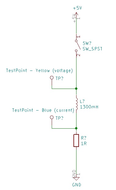
Any component that relies on an electromagnet or coil of wire for its operation will be inductive, that is the nature of coils of wire. Common examples are relays, solenoid and most types of motor.It is standard practice to put a 'flyback' diode across any inductive load in order to catch the back emf from the inductor when the current is interrupted. This requirement is usually taken at face value without being backed up by any kind of test results or evidence. This tutorial provides the evidence.
This is the test circuit without a a flyback diode. The 2 test points are where an oscilloscope was attached, the voltage test point (yellow trace) measures the voltage at the top of the inductor. The current test point (blue trace) measures the voltage across the resistor and therefore give an indication of the current through the inductor.
This is what happens when the current through the inductor is interrupted. This oscilloscope trace has the time base at 4ms per division for comparison to the trace in reply #1 with a diode in circuit.
This is when the current is being interrupted but this time the oscilloscope timebase is set to 80μs per division to make it clearer. Note that the voltage (yellow) is off the scale, which means it is well in excess of 200V.
You might ask why the current trace (blue) is also off the scale. First note that the input for the blue trace is set at 200mV per division, not 50V per division, so the blue trace being off the scale does not represent anything like what the yellow trace represents. That said I think it is because of the parasitic inductance in the test circuit allowing a high voltage to develop across the test resistance at the high frequencies that are present.
Note that not only is this circuit producing high voltages, it is also producing a lot of high frequency electrical noise.
Here's a better trace of just the high voltages and electrical noise, note that the voltage peaks are in excess of -300V.
Outstanding post, congratulations!
Being new to Arduino, I am very positive impressed with the community forum group.
Paul__B:
My point was that the inductor does not generate the transient; the switch does. The switch is in complete control of the voltage, and the transient does not emanate from the inductor, but from the switch.
The statement is correct.
In Electrical engineering, we learn that a sudden cut on the supply voltage, generates instability on the circuit.
Hence all the resistance, inductance and capacitance in the circuit impact during transient, and circuitry is added to ensure no damage occurs.
Professional businesses design their circuits and conduct several compliance tests.
Thanks also to Perry for bringing this important topic for discussion