Arduino nano v3 Solar pwm controller

Hi everybody, I'm new to this forum and to arduino as whole, but I'm pretty handy with electronics.
Ihttp://www.arduined.eu/arduino-solar-charge-controller/ wanted to build this circuit:

I build this circuit using EAGLE CAD but used the arduino nano instead of the mini that the project calls for.
here is the circuit I build:
Problem is that the circuit does absolutely nothing just sits there the led which is supposed to indicate activity remains lit and the battery remains at same voltage even when the solar input is connected and providing a higher voltage than the battery.

the only different parts I'm using is the 2 pnp transistors I'm using pn2907 instead of the 2n3906.

Thank you for your help

This is the code on the project:
const int setPoint = 13.5 * 20 / (20+82) * 1024 / 5;
int measurement = 0;
int pulseWidth = 0;
int difference = 0;
int stepSize = 0;
int calculation = 0;
int led = 13;

void setup() {
TCCR2A = TCCR2A | 0x30;
TCCR2B = TCCR2B & 0xF8 | 0x01;
analogWrite(11, 117);
analogWrite(3, 137);
// Serial.begin(9600);
pinMode(led, OUTPUT);
}

void loop() {
measurement = analogRead(A1);
calculation = setPoint - measurement;
difference = abs(calculation);
stepSize = difference;

if (measurement < setPoint)
{
pulseWidth += stepSize;
if (pulseWidth > 255) pulseWidth = 255;
analogWrite(led, 0); // pwm to LED
}
if (measurement > setPoint)
{
pulseWidth -= stepSize;
if (pulseWidth < 0) pulseWidth = 0;
analogWrite(led, 255); // pwm to LED
}
// Serial.println(pulseWidth);
analogWrite(9, pulseWidth);
delay(10);
}
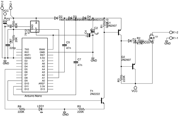
Here's the schematic the OP posted:

FYI: If you want to learn how to insert photos into the text [so it's easier for us to access/see it/them], read this: https://forum.arduino.cc/index.php?topic=364156.msg3749310#msg3749310

Also, it would be nice if you read, and complied with, the following, so you know to put your code in a code block, and such: http://forum.arduino.cc/index.php?topic=149015.0

And, a cursory look has me puzzled about T1. I'm not so sure pin 9 can turn T1 on enough to turn Q1 on. I would:

  • break the connection from D9 to T1 base, and insert a 470k resistor
  • Remove R5 and connect the emitter of T1 to ground
  • After breaking the connection from T1 collector to the Q1 base, move R5 to the T1 collector and Q1 base

That way, you will get a more solid switching action, there.

Also, the transistor substitutions should be fine: 2N2222 [PN22222 would probably be better] in place of 2N3904 and 2N2907, for 2N3906. Though, the 2N3904/6 have higher current gain at the lower currents involved. That might be an issue for T1 in the current configuration [to busy to analyze], but the modification I suggested should make it more immune to Beta spread.

Have you checked voltages and [if you have one] thrown a scope on those PWM outputs to see if they are swinging? Are you getting voltage multiplication at the Emitter of Q1 [what? Around 18 to 20V?]?

Also, you could write a test program that exercises, things like D9, and see if things are switching properly, and voltages are varying as they should. If you don't have a scope, then this can be a good way of slowing the action down, so you can use a meter [probably won't work for the voltage multiplier], but you might, at least, be able to verify switching at T1/Q1, and get a read on A1 and send it to a Serial Terminal, etc.

Thank you so much for your reply
Sorry one mistake on my schematic:
T1 is actually 2N3904 not 2N2222
This is the original schematic from the project.
Many people supposedly build it succesfully.

I'll try your suggestions for T1
And unfortunately I don't have a scope.

bigote:
Thank you so much for your reply
Sorry one mistake on my schematic:
T1 is actually 2N3904 not 2N2222
This is the original schematic from the project.
Many people supposedly build it succesfully.

I'll try your suggestions for T1
And unfortunately I don't have a scope.

Without a scope, troubleshooting something like this, is harder. Try my troubleshooting suggestions, and ask if you need more help [i.e. interpretation of readings, etc.]

I'm going to be "in" off and on, so I may not respond right away, but maybe someone else will pick up the slack.

T1 is use as constant current source.
When it's base is high (5volt), the emitter is 4.3volt, resulting in an emitter current (and collector current) of
4.35volt/220k = ~20uA.
That drives the base of T2 with ~17uA.
That results is a collector current of ~5mA (assuming β=300).
That drives the gate with 5mA.
T3 pulls the gate low when T2 is not conducting.

Not wise to use e.g. the 2N2222 here (lower gain).

The whole circuit depends on the voltage doubler generating a higher voltage than Vbat on C7.
Measure that first.
Leo..

Wawa:
The whole circuit depends on the voltage doubler generating a higher voltage than Vbat on C7.
Measure that first.

It occurs to me, bigote, if your meter has a low internal impedance, it might load down that voltage, and provide a false reading. For instance, a 1MΩ meter will, likely, give a reading that is lower than the actual voltage. A 10MΩ meter will get it nearly right.

Thanks to you guys for keeping up with me.
Wawa as I explained on my second post that is a typo on the schematic for T1 I'm using 2n3904 NPN same as 2n2222 but different pinout I also tried another transistor H9013 with same characteristics and the same results, no output from D9.
I did some testing with the PWM and POT sketch, and I can confirm the reading on the output pin using my tester so I know it works.
I'm using the popular Unity 139C multimeter.

thanks again

bigote:
... and the same results, no output from D9.
I did some testing with the PWM and POT sketch, and I can confirm the reading on the output pin using my tester so I know it works.

Did I miss something? I looked back at previous posts, and can't find a reference to what you're saying.
So, there's no output from D9? I'm lost :stuck_out_tongue:

Yes D9 remains @ 0 volts or very close to that. I even removed the transistor completely to measure this.
So I wonder could it be a software problem, knowing nothing about programming it would be impossible for me to spot the error if any.
regards and sorry about late reply

I did remove the 220k from T1 emitter and connected it directly to ground.

The output of D9 depends on battery voltage, so what is the voltage on C3.
And how much higher is the voltage on C7 (has been asked to measure that before).
Leo..

Thanks Wawa, the battery voltage is @ 12.8 volts small 12v 7AH sla batt.
It looks like part of the circuit is working voltage @ C7 is 14.5 and at D4-C2 point the voltage is 17 volts.
Yet at pin D9 absolutely nothing.
feel free to ask any other measurements.

If you connected emitter straight to GND you probably blew it AND D9.

Oops, I see you have named the parts differently from the original diagram.
That will lead to confusion.
C7 (electrolytic, 10uF) in the old diagram (C2 in yours) should at least be 10volt higher than Vbatt.

R8 in your diagram should be 1-10k (not 220k), so you can actually see the LED.

The 7812 is a poor choice.

  1. An 78xx is not low dropout, and needs at least 2volt across to regulate properly. 12.8 - 12 is only 0.8volt.
  2. The Nano is rated for 7-12volt, but people had clones blown up with 12volt.
    Could use an LM7808, or an LM7805 and connect directly to the 5volt pin (like in the original diagram).

Add some print statements, so you can see what is written to D9.
Leo..

1/

I see nowhere in the code where you set D9 to be an output:
You have to add pinMode( 9,OUTPUT); in the setup() part of your code. Otherwise you can't write to it.

Ditto for pins 11 and 13.

2/ I'd put a 1K between D9 and the base of T1 and ground it's emitter.

Allan

Code source.
No pinMode calls in setup()... :o

allanhurst:
2/ I'd put a 1K between D9 and the base of T1 and ground it's emitter.

That could fry the base of T2, and/or load down the voltage doubler.
As said (post#4), T1 is used as constant 20uA current sink.
Leo..

Then add a 10k in series with it's collector as well.

20uA seems very small even with the gain of T2 if you want to switch a big MOSFET reasonably quickly - 3-5nF gate capacitance or more ?

suppose the gain of T2 is 100 - optimistic. Then the turn on current is only 2mA.

this means that with 5nF I = C dV/dT -> 0.4 V/uS, and to traverse 10 volts will take 25uS.

Pretty slow.

At 1kHz PWM this means 50uS spent in transitions per 1ms cycle or 5% of the time - a significant loss.

Allan

D9 is ~500Hz PWM, so one transistion per 1ms.
And from non-conducting to almost fully conducting is not the full 10volt
But there is indeed some loss there.
If that's a problem or not depends on the output power of the panel.

Gate current(s) could be increased by lowering the value of R5 and R3 to say 100k.
And maybe removing (short) R2. (Parts numbers of OP's diagram).
Needed or not depends on the gate charge of the actual mosfet used.
Leo..

I believe the analogWrite function takes care of pinModeing the target pin, but, does the pin return to input after the analogWrite is finished?
This works on a Pro Mini:

void setup() {
  
}

void loop() {
  for(byte i = 0; i <= 240;i+= 10){
    analogWrite(6,i);
    delay(200);
  }  
}

Changing a PINMODE is handled by the Analogwrite() function... but once set... it leaves it that way. It will not change back to default INPUT mode when the function call is completed.

bigote:
Yes D9 remains @ 0 volts or very close to that. I even removed the transistor completely to measure this.
So I wonder could it be a software problem, knowing nothing about programming it would be impossible for me to spot the error if any.
regards and sorry about late reply

I did remove the 220k from T1 emitter and connected it directly to ground.

When you did this, was a base resistor fitted to the transistor?
If you did not have a base resistor fitted, then you could have damaged the pin9 output because the 0.6V Vbe of T1 would have clamped the output pin when it was trying to output 5V.

Modify your code to control another unused PWM pin on the Nano and try it with T1 removed.
Have you made a PCB for this project?
Can you post an image of the CAD for the PCB?

Thanks.. Tom.. :slight_smile: