Building MCU/computer, help needed! =)

Okay, this is my first post and my English isn't the best. because of that , example, some part or whole post can influence ridiculous.

But for the main point of my post. My idea is to build simple stand alone
microcontroller interface with input interface with buttons and at least two 8x8 one-color led matrix to output display(for debugging some leds are okay in for start now, and it will be final device to design more complex display interface, but not LCD with already complex 1/0 build interface build in it)

It wont't need any outside CPLD device, example Arduino (that's optional for now , but my it is final goal, there will be maybe some ports to allow communicate with pc, trough USB interface ) , so it has to be finally capable to build some simple applications, for only its own with custom build button interface.

For now, I have to find most realistic windows based FREE application to graphically simulate it and/or at least program to allow user build some kind of clear component/connections/output/input/code tree to debug it with very realistic electrical laws. Not logic only.

Some logic simulators have good for logic and I have designed complex system with them , but those are usually only for logic, example logisim does not have electrical components with specific electrical value range and those lags for proper interface(example resistors, only 1 pin and no resistance. value).

Next thing, which I wanna start in, is the whole hardware structure. (and suppose I have to learn/debug hardware in the same time just with main components at least).

I already have many many 4000 series chips, and some 7400 series chips, most recently have purchased some more complex ships, I have one MAX led driver coming soon(which I don't think it's enough to the whole display, for driving all the leds).Sorry I don't remember that's part name.

I Also have two Motorola's CMOS 4000 series 4-bit ALU's (74181) which I will use in the ALU and I will add more complexity maybe to make them more functional capable. Here are some questions about those alus, I have many 7400-series based 4 bit full adders and basic gates and 400-series based 4013 chips(dual flip flops) , can I make those two 4-bit alus much more capable to execute more complex functions and how to compine them? What about connecting ALU to others CPU's units, do I have to develope some other complex chip from bunch of CMOS gates, counter etc, example, for connect every unit in the CPU? Which are the most cricital , and important other CPU's parts, exept ALU, which will be important to start developing now?

I have two SRAM chips part named HM6268P-35 which both have 4096 Byte of Static SRAM TTL compatible memory , for each.

Then I have one Winbond W29C040-90, named, preprogrammable (with 5V programming voltage, 12V is no needed, which datasheet says.) It's memory capacity is 8x 512KB which all is shared for units which each contain 256 bits.

All those memory chips and both ALU's are pin compatible for prototyping them in breadboard, so what is number one thing and the information which O have hard time to find answer is can I use arduino mega 2560 to program the flash chip? What's the hardware programming schematic/connection diagram to arduino and need some code...That winbond chip contains already some programmed areas. Datasheet says there are some logic device inside it too, not memory only that's is etc. logical unit for erasing, programming etc. buffer. Memory already have too 16KB boot-ready sector

And there is too option to which lock some basic most important functions of use the chip. To write specific hex code combo when programming, the chip set some kind of short combo of short code in, that's full function I don't remember, but there is risk that option can accidentally set on. And then there will be very hard to find to way to set that option back to off.

So Two sram...can i use second one to register and the other for RAM? And Program The flash chip so, that there will be bigger non violable sector for programs and same some areas will be critical for CPU , and there will be information to basic CPU functionality and so the whole cpu system can work with all requirements example to execute some functions to cover hardware from damaging, if there appears some serious errors in code?

The flash memory can have too some kind of bios for booting and changing most critical system configurations as well?

Greetings everybody, who's are interest to help. My knowledge is hard to explain , although I have some of pretty advanced knowledge from hardware based things, my self learned knowledge of everything about programming( I understand averagely/good, design like beginner most of most usual languages)is pretty messy and unbalanced, so there is holes maybe in some basic things of my hardware skills. I know basic things in electricity good/averagely but again, I have often noise problem in more complex breadboard based circuits and 555 based oscillator circuit won't do them any better , but harder to filter.

Again I thanks for everybody for help and sorry if my text is messy and harder to read.

If I got enough help there, I will put every working schematic and diagrams here, I promise =)
Spice might help with the simulation but something as needlessly complicated as this will quickly exhaust the limitations of the free ones.

Thanks from your answer!

I'm going to purchase some software, in near future, but for now I need at least some with decent trial period. A good example is that I yesterday tried some java, i suppose , based application to design circuits, but it had only 3 day trial period!

Does anybody know everything about using Arduino, to program FLASH memory chips? It needs 5 volts so external 12V isn't needed.

And if somebody know, if there's any logic simulator, to already have 74181 model, have somebody built any model in logisim and wanna share their model? (.circ file)

Also some only logical ones, design,simulation or simpler practicing tools for CPU design would be handful if not so extremely simplified.

Anyone ever built anything from 74181 ALU? Please share your schematics and/or experiences for me if you wanna.

I know my project will be complicated, but main things of CPU first, connections, buses (The flash memory questions) are most important for now, and Yes the flash mem too because if I store there some data that CPU needs to work properly.

I used the 74181 ALU 30 years ago, and have no desire to even try to remember any of the details.

Ok. Thank for your answer anyway.

The TI data sheet for the 181 has an MSI equivalent you can use to build up a model from logic gates.

Thanks! TI data sheet looks much better than the previous datasheet of 74181 or actually MC14581CL so it's both ALU's which I have are Motorola's version of CMOS 4000-series version of 74181. And haven't find yet exactly the original datasheet for them. The whole pack of chip of each ALU, have some gold painted look, hope there is no any Pin differences, VDD and VCC seem to be right thought and so both pin side of 74181's inputs and outputs, tested them with low voltage and leds and same time I looked the 74181 truth table. For Pins everything seems fine so far, 5 output in VDD side of pins and three output in VCC side of pins and function seems to be same as TI datasheet, example.

I actually have already built 74181 model in logisim, but haven't fully tested it's functionality vs real life chip. That's because that's actually pretty old logisim simulation only project where for some reason I stopped developing more. I will try the model , if it's all logical and arimetrig functions are working properly.

There one stupid simple question. When I opened the models which have some negated buffer missing and instead them there are one buffer and one inverter, so looks like I can't even do negated buffer in logisim, but how do I replace them so they have same function....I now basically what is buffer gate, but why exactly there are negated buffers in 74181 ALU?

Probably for timing reasons to keep the same number of logic gates in each path.

OK, thanks again, seems like 74181 outputs/inputs need transistors and/or resistors because opposite to some other 4000 series cmos chips which many(probably newer ones and from different manufacturers) have equal voltage/current value in them outputs, at least this cold painted Motorola's MC14581CL flash leds differently, some flashes brighter and some stay darker when the output's value is constanted 1, there is enough difference to easy burn some led, if not use at least proper value resistors.

Surprisingly, all outputs of my old logisim model of 74181 seems give right value, when input is constant. Just checked that in my breadboard and compared to logisim 74181 model same time. Maybe the negated buffer works in same way as 0/floating inverter + 0/1 buffer but it doesn't need so many transistor as inverter + buffer?

So for now, I at least give old good logisim a try. Same that developing the whole computer is maybe more complicated with logisim , what comes to the newer memory chips which i have, which are naturally much much more complex and therefore I think that's way there is not even logic diagram available public with every singe gate memory's decoder or control unit are shown, or are there any standard logical design for reprogrammable flash memory chip? I mean row decoder etc, things that matter when simulating real life things. not every single gate is necessary show for memory shells itself. I know there is flip flops, Although I don't be sure if they are nand or nor gated.

In logisim there are blocks which are called memory , but I'm curious if they do the right job in my case. I try to avoid using too much extra stuff if I use them. There are not enough big memory units in logisim, to demonstrate my SRAM chips, I have to combine them and I think that's not so good idea.

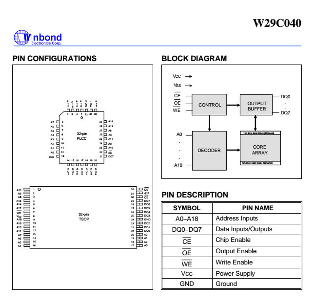
My sram chip datasheets have clear picture where is some logic gates and row decoder etc...so everything seems to be like any basic ram memory chip schematic, but Winbond chip datasheet circuit schematic only shows very simplyfield diagram of logic gates here is picture from datasheet where is pin configuration too(from some reason there is now pin configuration for DIP package..)

![|403x500](http://http://snag.gy/cJ7K7.jpg
Here is sram chip's logic diagram as well:

)

Here are both memory chip's pin configuration and schematic

have some prolems using online image editing tools