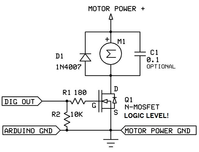
It is my understanding that R1 is most significant in frequency applications (due to Gate capacitance C1)
For very low frequency applications (less than 1hz) it limits the current flow to and from the gate.
As the PCF8574 has limited drive capabilities (4ma), I have chosen a value of 1.5kΩ.
R=E/I R= 5v/4ma = 1250Ω
AM I INCORRECT? (you may now proceed with the slings and arrows)
1.5K is a reasonable choice for 4 mA maximum instantaneous drive, but the manufacturer of the PCF8574 recommends 1 mA maximum (presumably steady state).
NO!
A floating gate means the gate pin is left unconnected, or its voltage is not firmly controlled.
The MOSFET gate is a capacitor—if left floating, it can accumulate charge from stray signals or ESD.
This can cause the MOSFET to:
Partially turn on, leading to unpredictable behavior.
Oscillate or heat up, especially with inductive loads.
Fail due to excessive drain current or thermal runaway.
My recommendation is leave R2 in and place it on the port side of R1 as indicated by @jremington
I don't think OP's question was about whether the input should be left floating, it was about whether the sole purpose of R2 is to drain the gate-source capacitor if/when the input is left floating.
I have seen many examples both ways. I do not think it makes a discernible difference.
In my configuration instance the gate is looking at 100k to ground and the input is seeing 101.5k to ground.
In your configuration instance the gate is looking at 101.5k to ground and the input is seeing 100k to ground.
Am I missing something?
Apparently. The "wrong" way is a voltage divider that lowers the gate drive voltage. In many cases, correcting that error may not make a discernible difference in performance.