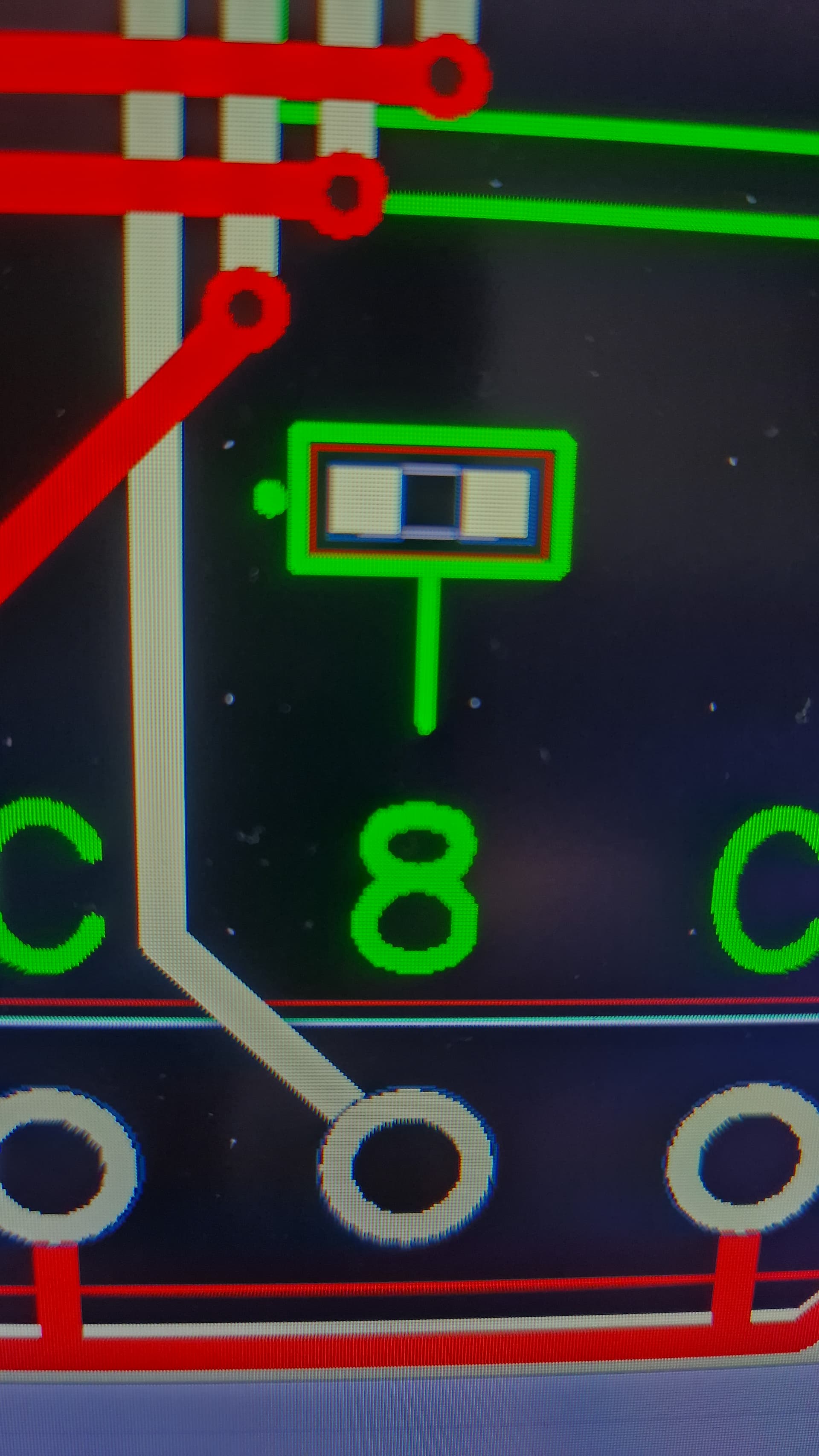
Usually the dot indicates pin 1. However, there is no fixed convention as to which is pin 1 in this type of footprint, nor is there a standard for which pin is marked on the actual device, it even varies for a single manufacturer.
I guess the most widespread convention is to mark the cathode on the device (same for polarised capacitors, and through hole devices). Pin 1 is often assigned to the cathode. That results in the device marking aligning with the PCB marking.
However without the schematic - footprint mapping, I think the only way to tell for sure is by examination of the circuit.
I mean really..... why can't these chumps get some kind of alignment on this stuff.
The different naming and symbols for devices, footprints etc drives me mad.
D2 illustrates what I mean: R1 sees D2's cathode as positive and D1's anode as negative, hence the labelling. However, while I have often seen a + next to the cathode as on D2 I have never seen a - next to the anode as on D1, but I included the - for completeness in the illustration.
Of course, voltage or potential difference is relative. Normally people pick a 0V reference relative to the voltage source and call it "ground", but if you choose some other arbitrary reference point I guess that is up to you. Seems like a pretty weird thing to do though.
At the risk of straying too far away from @baffled2023 's original question:
The individual components only see what they are connected to, they know nothing of 'ground' or '0V' or anything like that, just what their wires go to. In my illustration R1 only sees D1 anode and D2 cathode. There is no ground because I have not designated one. If you read forum questions you can see examples of new folk falling into the trap of, for example, thinking they can use an NPN transistor as a high side switch 'because they are putting 5V on the base'. The 5V is with respect to 0V, about which the transistor knows nothing. The transistor responds to base -> emitter current, and in this case tries to conduct until the emitter is at about 4.4V with respect to ground, or rather -0.6V with respect to the only thing it knows about: its base voltage.
So, I suggest that it is not:
It is what you need to do to understand the circuit.
I understand your point, however it could easily be misleading. If you measure across each of the diodes, both will have the anode at a higher voltage than the cathode.
I agree, but I was illustrating something I've seen many times and the rational behind it.
I agree that it is functionally equivalent but it doesn't illustrate the point I was making. The circuit I posted was deliberately simple to make a point. You could add more complexity to my circuit so that it could not be simplified as you suggest, but then that would obscure what I wanted to show.
Without trying to see as many schematics as there are, I did spend some time looking around.
Diode symbols when they are not in a schematic but are labeled show the positive sign at the anode and the negative sign at the cathode.
The cathode of a diode is often, but not always, the one marked on the device package. The flat side or the short leg or a band, whatever.
I think I got a question wrong on a test somewhere because I couldn't look at the insides of a LED and see from the structure which be which.
There is one place where + and - do show up on the "wrong" side, and that is when configured as a full wave rectifier, or other kind with two diodes and three legs.
Needless to say, I usually test LEDs for function and pinout.
Needless to say, I still manage to install them backwards.