Well, I've had these 2560 boards on hand for a while now, finally got some chips on hand (seemed to have misplaced the last pair I ordered) and the right crystals (CTS406), so got brave yesterday and tried assembling one.
We assembled the bottom parts & reflowed them. So far so good. Put some kapton tape over the crystal just in case capillary action didn't hold it in place.
Stencil from pololu.com was no good, had several tear out between pads. Luckily I had a metal stencil from
www.proto-advantage.com I could use for the chip.
Getting the paste on the 2560 pads was a challenge. Would miss by a couple, would get the paste between pads, would leave some pads uncovered, would be slightly twisted. Took me about 6 tries to get them covered satisfactorily.
While I was doing that, Kathy (MrsCrossRoads) was practicing placing a part on a unpasted board.
Finally got the 2560 in place, added the DTR cap, and back to the reflow oven.
Couple minutes later, card was cooling off and looking good.
Added a few headers - 5V enable from FTDI header, FTDI header, DTR enable, and ICSP - connected up an FTDI Basic and Atmel AVR ISP MKii, and Bootloaded! You can see the end result on screen behind the part.
Also downloaded Blink to make sure the Serial port was working.
Got a couple more ready with parts on the back, will try them after we get some lunch.
At $15/processor chip (10-lot price) I am sure glad this worked!
Also buzzed from each pin at the body to the pads to make sure each pin was soldered down.
Looks quite beautiful. Now it's time for you to try the ATmega2560-16CU. Perhaps MrsCrossRoads could do the trace routing...
I don't think so. Really need 4 a layer board to be able to get all the traces out with BGA, I try to keep things on just 2 layer to keep PCB cost down.
Do you think it would be practical to just bring out the "interesting" pins using 2 layer? The Arduino Uno pin 1-13 and A0-A5 assignments, plus a handful of additional pins like SPI and Serial1, Serial2, Serial3? Or is doing that still a job for more than 2 layers?
Don't know, need to find a BGA footprint and see what's possible.
One thing I forgot - I started looking at this board as a way to drop in a replacement processor on a Mega without needing reflow soldering. By putting most of the support parts on the bottom, this looks like that could be possible.
I was hoping for a drop in replacement for the ATmega328P on Uno or similar board. 28 machine pins sticking out the bottom of the board to plug in to a DIP socket, and 2 rows of pads on top of the board where wires or pins could be optionally soldered, for example to access extra serial. Here is a fantasy mapping attached. First text in each cell is the ATmega2560 function, second text is the equivalent Arduino pin mapping on ATmega328P or 2560, and third row is what DIP pin it goes to. In the third row y and z represent the extra pads on top of the board. What do you think?
map.pdf (38.4 KB)
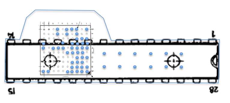
A rough idea of what a BGA ATmega2560 would look like sitting on a board that fit ATmega328P socket. I was picturing using the "postage stamp" edge to solder the machine pins to, for all but about 6 of the pins. The 6 pins underneath the ATmega2560 could be shaved off with a moto tool to make them surface mount.
Seems like you'd want the SPI pins and I2C pins as part of the 28, not as optional pins. Also Rx0/Tx0 which I don't see listed.
Okay PE0 & PE1, going to 328 2 & 3, that's good.
Yeah, I don't know what's better, put the 2560 SPI on Arduino pin numbers 11, 12, and 13, or preserve the Mega2560 pin numbering and put the SPI on the extra pads. There are benefits/drawbacks to either way.