Rather than use wire jumpers, I sometimes use zero ohm SMDs (1210 & 2010) to sneak over a trace.
Rather than going back to the schematic, adding the resistor then recreating the net list;
any suggestions how to add them to the layout to still pass the DRC test in PCB layout?
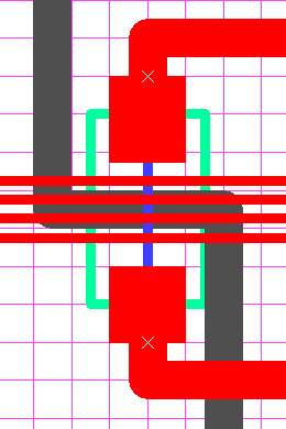
(perhaps two vias with oposite side trace is the only way)
I use WinQcad but the concept would be the same as other programs.
LarryD:
(perhaps two vias with oposite side trace is the only way)
It has the advantage of showing the intent and actually being valid as a 2-layer layout.
What you want is a way to automatically add pads to the vias. If there's a way in WinQcad
to create a window in the solder-resist that would do it - perhaps some sort of test-point?
In Altium I would create a pad as a component (I already have many different ones I use for test points) then drop two on the schematic.
But how to do that on the PCB and have it back annotate to the schematic I don't know, not even sure if it would be possible. I think it would be just as easy to swap back to the schem and drop the pads as required.
Come to think of it, if you etch the top and bottom of the PCB (assuming no platted through holes) a middle or imaginary layer can be used to satisfied the DRC using the same technique.
See image: