valmishra:
I am not sure to understand what you mean. If I understand correctly:
A 24bits ADC would output 24bits*sampleRate per second.
At a sample rate of 3kHz this would bring us to
72k bits/sec.
That's quite close to the usual 100kHz of SPI clock. That clock can be set higher, provided that the connection supports higher clock rates.
But then you run into another timing problem, because you most probably want to get values at a fixed sample rate (constant time increment), with no missing samples. The external sigma-delta ADC are free running, with no settable conversion rate, so that every sample must be requested at the right time. This requires the use of timer interrupts, for the start of a transmission, and possibly SPI interrupts for reading the remaining bytes. Concurrent interrupts (time, communication...) can introduce random delays.
Next comes writing the values to external SRAM, by SPI or I2C, that introduces another delay and possibly further interrupts. You can find out yourself, how fast an accurately timed acquisition is achievable, once you have all hardware connected. Use e.g. a precise triangle wave generator and check the returned values and peaks for equal distance, and the correct number of samples within a given time frame. Then you can find out how many of the 24 ADC bits will be undistorted.
I really don't want to discourage you, but you should know which items require special care in your project.
That's quite close to the usual 100kHz of SPI clock. That clock can be set higher, provided that the connection supports higher clock rates.
I would accept that comment if we were talking about I2C but not SPI. Most SPI devices work at 1MHz or above with only the occasional one requiring 500KHz.
Given you only have 2K of SRAM on a Uno you either can only sample a short time or you need an external RAM. The problem is you have never said how many samples you want to store and what you are looking for in this signal.
I would forget I2C devices they are simply too slow at these data rates. Then there is the other "problem" that you have not specified what you want to do with this data once you have it.
The whole project needs a lot more thinking about before you place any orders.
This is very valuable information thank you DrDiettrich and Grumpy_Mike!
-So if I understand correctly SPI should be fast enough.
-About the number of samples and memory: I though about doing a Daisy-chain from ADC_output to the SRAM-input. Once the SRAM will be filled I will stop the acquisition and read the data. This way I am saving a read/write cycle from the Arduino.
-I intended to "time" all the measurement using the SPI masterclock (I need equally time spaced acquisition indeed).
Totally off.
You can not get an A/D to talk to a memory chip directly, you need a processor in between.
The concept of timing anything from the SPI clock makes no sense at all. What do you mean?
You still have not addressed the questions about sample rate and how the data will be handled once acquired.
I haven't looked at the datasheet, so one more byte might need to be sent out to set up the ADC, or the data might need different manipulation to put it together.
Grumpy_Mike:
Totally off.
You can not get an A/D to talk to a memory chip directly, you need a processor in between.
The concept of timing anything from the SPI clock makes no sense at all. What do you mean?
You still have not addressed the questions about sample rate and how the data will be handled once acquired.
I though I could just send the bits from the ADC ouput into the SRAM output (in sequential write mode). Too bad.
Timing with the SPI clock: I would like to get equally spaced samples using the clock. That is the ADC will output a measurement every X clock preiod. I do not need to know absolute times, all I want is the time interval between samples. I though SPI clock would do the trick ?
About the data handling: I will fill the SRAM. Once the SRAM is filled, I will stop the acquisition and take all the time I need to read the data with the Arduino, send them to the PC and then do some analysis.
No to do this you use the system clock and one of the internal hardware timers, then the interrupt will be triggered at a regular interval. The interrupt service routine then takes the sample.
The SPI clock only goes in bursts of 8 pulses so I am not sure how you got the idea it would be suitable for timing.
I will fill the SRAM. Once the SRAM is filled, ...
So that implies you know the size of the SRAM, they come in various sizes and you still have not said about the sample rate.
Wow it sounds like I really need to do some digging on SPI and timing. Since I do not have the hardware available right now it is difficult for me to realize when something is not right, I'm better at trying stuff. Your inputs are really appreciated.
SRAM:
I'm thinking of using the 23LC1024 SRAM chip which is well documented, works with the Arduino 5V and seems very popular. It also has a massive memory (1Mbits).
Sample rate:
the signals to sample will range from 0 to 1kHz.
So my sample rate will need to be higher than 2kHz. For the moment let's say 3kHz to be safe.
So I though the workflow would be:
repeat every 3ms (3kHz) {
1)take a 24bits sample from the ADC
2)transfert the 24bits to Arduino buffer (SPI)
3)transfert the 24bits to SRAM (SPI, sequential write)
4)empty Arduino buffer
}
5)Stop the process when XX bits are in the SRAM chip
eg: for 2seconds worth of data it would be 2s3kHz24bits=144'000 bits
6)Transfer these bits to the computer.
7)repeat from 1.
Once the chip is filled I will just write on it from the beginning (first adress) or erase all bits on it. But this is an other matter.
Sequential write seems the way to go since there is no need to input addresses after the first one (that is the reason why I though I could daisy chain the ADC and the SRAM). Obviously I was wrong;).
The crucial thing here is the timing: I though the SPI clock would allow me to to properly time the 3ms loop I mentionned above.
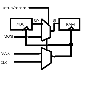
SPI RAM indeed should allow to take large samples at high speed. After the initialization sequence (write command and start address) the data can be clocked out of the ADC into the RAM, as fast as the ADC allows for. Slower is possible as well. Simple electronic is required to switch the RAM data input (SI) between the controller and the ADC SO.
Which is 128K bytes and with 3 bytes per sample is 42K samples.
Which is just about a second at CD quality rates. So not so massive.
Sequential write seems the way to go since there is no need to input addresses after the first one
Yes but there is a problem here. If you use sequential writes on the memory connected to the SPI bus then you can not also connect the A/D on the SPI bus as well. This is because the chip select on the memory going high finishes the sequential operation. It needs to go high to talk to the A/D.
that is the reason why I though I could daisy chain the ADC and the SRAM
Just think, what in the A/D is going to manipulate the lines on the SPI interface of the SRAM when the sample is ready to transfer?
So my sample rate will need to be higher than 2kHz. For the moment let's say 3kHz to be safe.
You still haven't said what you want to measure on this signal. For some measurements this is not high enough.
DrDiettrich:
Chaining multiple SPI devices is standard technology. I don't see why it shouldn't work.
It is not chaining it is using multiple devices on an SPI bus.
Did you not read the bit about the sequential addressing mode?
Sure you can use both devices on the SPI but but you can't have the memory working in sequential addressing mode, like the OP was going to do. The only sequential addressing you can do is with the three bytes for each sample.
DrDiettrich:
Simple electronic is required to switch the RAM data input (SI) between the controller and the ADC SO.
Once the start address is configured, the input can be switched to the ADC output, then both devices are enabled and the data is transferred at SCLK speed. The SCLK pulses can be forced by dummy SPI.transfer calls, or by any other clock source.
Basically I can't see how this will work. One problem is that any command to the A/D will cause that command to be stored in the memory eventually, but there are other things I am struggling with. So a schematic would help me understand. If I am having a struggle to envisage this then I am sure the OP will not understand this configuration.
Been looking at this for a few days and I can't make it work in my head. It needs to be a lot more complex than this. You can't just use 2 input data select blocks.