Can someone point out the error in my assembly code?

int a0,a1,b0,b1,F;

void setup() {
  // put your setup code here, to run once:
  pinMode(2,INPUT);
  pinMode(3,INPUT);
  pinMode(4,INPUT);
  pinMode(5,INPUT);
  pinMode(8,OUTPUT);
}

void loop() {
  // put your main code here, to run repeatedly:
  a1 = digitalRead(2);
  a0 = digitalRead(3);
  b1 = digitalRead(4);
  b0 = digitalRead(5);
  F = (a1&&!b1)||(a0&&a1&&!b0)||(a0&&!b0&&!b1);
  digitalWrite(8,F);
}

I am trying to implement the same code in assembly language and have written this code but for some reason it is not working.

.include "/home/sophia/FWC/main/assembly/setup/m328Pdef/m328Pdef.inc"

; Identifying pins 2, 3, 4, 5
ldi r17, 0b11000011
out DDRD, r17

; Activating pull-ups
ldi r17, 0b11111111
out PORTD, r17

; Declaring 8th pin as output
ldi r16, 0b00000001
out DDRB, r16

start:
  in r17, PIND ; Reading the data from pins 2, 3, 4, 5

  ; Taking a0
  ldi r24, 0b00000100
  mov r18, r17 ; Copy content of r17 into r18
  and r18, r24
  ldi r25, 0b00000010
  loopa0:
    lsr r18
    dec r25
    brne loopa0

  ; Taking a1
  ldi r24, 0b00001000
  mov r19, r17
  and r19, r24
  ldi r25, 0b00000011
  loopa1:
    lsr r19
    dec r25
    brne loopa1

  ; Taking b0
  ldi r24, 0b00010000
  mov r20, r17
  and r20, r24
  ldi r25, 0b00000100
  loopb0:
    lsr r20
    dec r25
    brne loopb0

  ; Taking b1
  ldi r24, 0b00100000
  mov r21, r17
  and r21, r24
  ldi r25, 0b00000100
  loopb1:
    lsr r21
    dec r25
    brne loopb1

  ldi r22, 0x00
  ldi r23, 0x00
  ldi r24, 0x00
  ldi r26, 0x00
  ldi r27, 0x00
  ldi r28, 0x00


  ; POS expression
  ; F = a1b1' + a0a1b0' + a0b1'b0'

  mov r22, r18 ; r22 = a0
  mov r23, r19 ; r23 = a1
  mov r24, r20 ; r24 = b0
  mov r26, r21 ; r26 = b1
  com r26
  com r24
  
  and r23, r26  ;r23 = a1b1'
  
  and r22, r19  ;r22 = a0a1 
  mov r27, r22
  and r27, r24  ;r27 = a0a1b0'
  
  and r24, r26  ;r24 = b0'b1'
  mov r28, r24
  and r28, r18  ;r28 = a0b0'b1'

  or r27, r23
  or r27, r28

  out PORTB, r27

  rjmp start

Can anyone please point out the mistake?

(P.S. I am new to assembly so a little explanation would be great)
Please explain what "not working" means. What did you expect to happen, and what happened instead?

It is an EXCELLENT idea to use parentheses to make sure that you and the compiler agree on the order of precedence and operations, for lines like this:

  F = (a1&&!b1)||(a0&&a1&&!b0)||(a0&&!b0&&!b1);
2 Likes

avr-objdmp is a great tool for seeing how the compiler does its stuff

1 Like

Yeah sure, btw I had earlier uploaded the wrong assembly code. It is updated now.

While verifying the output with truth table, I am getting incorrect output for a0 = a1 = b0 = b1 = 1.
It should give 0 but it is giving 1.

Can you give any references on how to use it?

"avr-objdmp -?"
will tell you all.

1 Like

The output of what, exactly?

If you mean the line of C code that I quoted, you and the compiler evidently don't agree on what it means.

Sketch #1 shows setup() configuring pins 2, 3, 4, 5 as INPUT and 8 OUTPUT.
Sketch #2 shows DDRD pins 2, 3, 4, 5 as INPUT (0) and 0, 1, 6, 7 as OUTPUT (1) (right-most is bit 0)

1 Like

If I could offer some advice:

  1. name your registers. #define a0 r18 is fine. ".equiv a0,18" if you're avoiding the C preprocessor.
  2. there's an immediate form of the and instruction (andi), useful for accessing bits without using an extra register. (only works on high registers, but that's all you're using.)
  3. Don't use binary constants for integer values of loop counts. (and I think that's your mistake - when you get b1, you're shifting by 4 instead of 5.)
  4. maybe check out the BLD and BST instructions.
  5. COM compliments all the bits. Since you're generating booleans, that's undesirable.

No, that is giving the correct output. The assembly code is not working.

; Declaring 8th pin as output
ldi r16, 0b00000001
out DDRB, r16

But I have declared 8th pin as output here. Shouldn't this work?

Well how do I solve the problem you mentioned in point number 5

That "1" is bit zero/LSB... reading right to left.
(Mitch Davis on YouTube has a nice series introducing Arduino register programming)

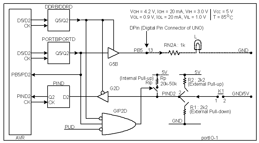
You have stored 1 (HIGH) at Bit-0 of the Port-B's Data Direction Register.
So, Bit-0 of Port- B (PB0) will work as output pin and it is has been marked as DPin-8 on the edge connector of the Arduino UNO Board.

Why not -- using "bitwise &/|" instead of "logical &&/||" as you are getting either 0x00 or 0x01 in response to digitalRead() and declare data types of the variables as byte instead of int for easy reading/evaluation.
F = (a1&!b1)|(a0&a1&!b0)|(a0&!b0&!b1);

Excite 2, 3, 4, 5 with LOW, HIGH, LOW, HIGH (mind that you have internal pull-up resistors enabled).

==> F = (00 & 01)|(01 & 00 & 00)|(01 & 00 & 01)
==> F = 00|00|00
==> F = 00 (LOW)

Should be --
pinMode(2, INPUT_PULLUP);

as you have enabled the internal pull-ups in the following assembly codes:

; Activating pull-ups
ldi r17, 0b11111111
out PORTD, r17

This topic was automatically closed 180 days after the last reply. New replies are no longer allowed.