How is the DUE I2C wired? I've read the schematic, but when I ohm out sda1/scl1 (the first two pins near the reset button) with sda/scl pins (20/21) they dont connect. However, the same pairs of I2C pins are directly connected on the Mega2560. I've found that an RTC (i2c address x68) will work on DUE pins 20/21, but not scl1/sda1. Is there an address namespace problem here? Should an I2C work on either I2c buss on the due? I understand one is 3.3 and the other 5, but the same i2c device works on one bus (scl/sda) and not the other (scl1/sda1).
Might be worth looking at the schematic;
They are a second independant I2C port, so not connected to the one on pins 20,21.
According to this page
TWI 1: 20 (SDA) and 21 (SCL)
TWI 2: SDA1 and SCL1. Support TWI communication using the Wire library. SDA1 and SCL1 can be controlled using the Wire1 class provided by the Wire library. While SDA and SCL have internal pullup resistors, SDA1 and SCL1 have not. Adding two pullup resistor on SDA1 and SCL1 lines is required for using Wire1.

SCL1 and SDA1 don't seem to the shown on the pinout diagram above, but they are not near the reset button.
Those pins should be connected, but they are not SDA1/SCL1, they are just SDA/SCL.
EDIT:
This pinout has the pins near the reset pin labelled as SDA1 / SCL1:
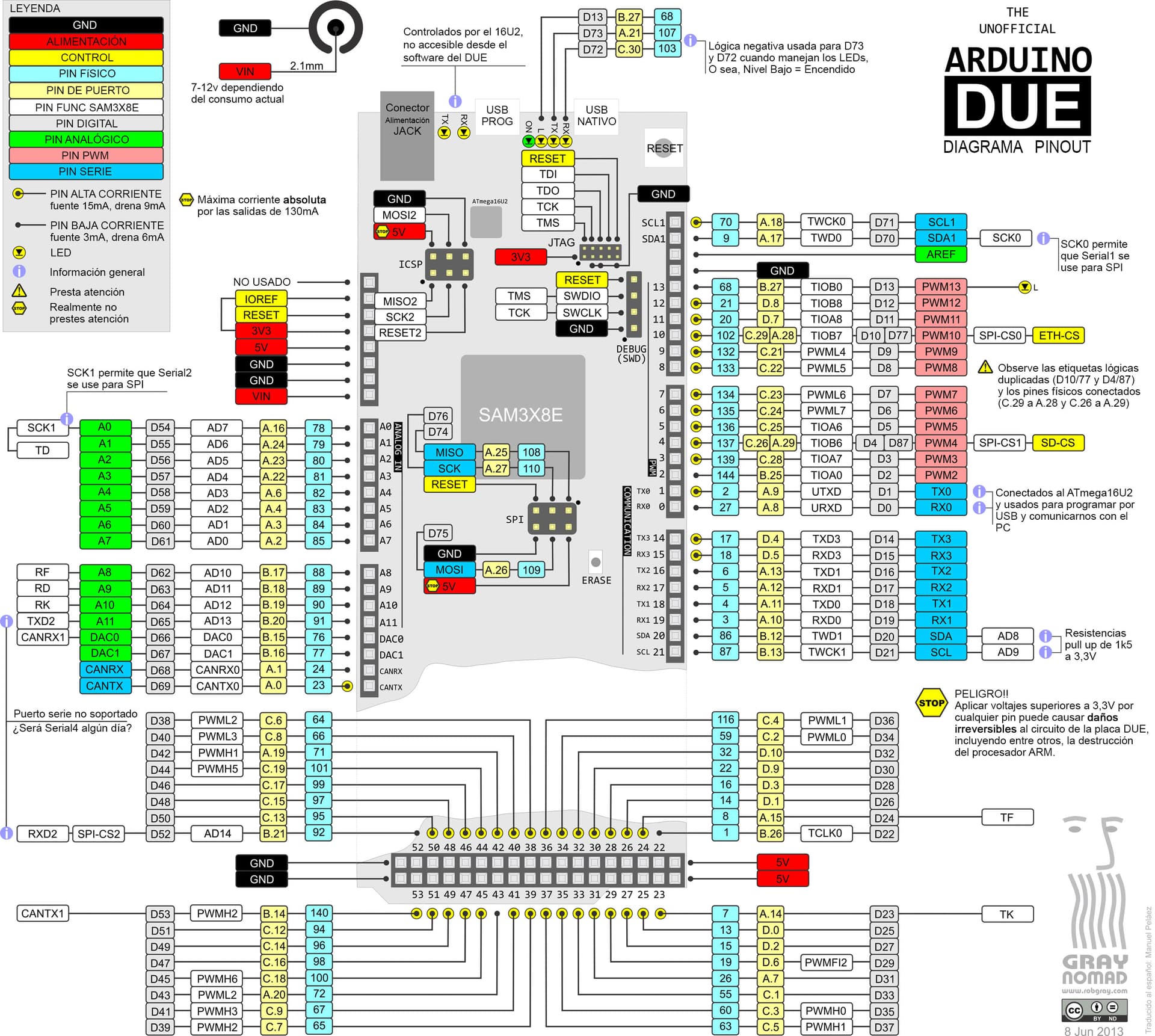
This explains why they are not connected to pins D20/D21. It also means that the pinout diagram on the official Due page is incorrectly labelled!
Makes sense. Thank you. I wonder if using "INPUT_WITH_PULLUP" pin type is appropriate for SCL1/SDA1. Otherwise, I suppose a bodge is called for.
This topic was automatically closed 180 days after the last reply. New replies are no longer allowed.