These are the type ssr I have used before. They are awesome, but they are also significantly bigger than the mechanical relay I am contemplating using. I used brand “songle” in my description of the relay. I guess that may be a bad choice of brand. I have read many users that are not fans of their relays. But they are very popular and most people have heard of them which I thought made it easier to understand what kind of relay I was talking about. I have no preference of brand in this case. So, maybe I should be looking for a better brand relay with a similar PCB footprint. One that is ACTUALLY believed to handle the current that is printed on it. You apparently believe the songle relay, although has a written current rating of 10A only will actually handle a fraction of that. So is there a better brand mechanical relay with a better foot print?
For grins and giggles, several days ago prior to posting this thread, I did connect one of the relay breakout boards that I have on hand that has the songle relay attached to a MUCH higher load (1500 watt heat gun) than I ever plan to use. This exceeds the current rating of the relay, but I wanted to see how it held up. And it seemed to do fine.
Now, I am not arguing the point with you. I understand this is one relay, tried one time, not in a controlled environment, a resistive load, not an inductive load, not tested after 1000s of arching on/off events etc. but the one relay did what it claims able to do.
These kind of relays (not necessarily brand) are used on tons of PCBs designed by engineers and are ul approved. So, they can’t all be bad, and some have to be capable of what they claim. Which ones are those? I want to get good quality hardware! I know Sony makes similar style relays and I’m sure there are others. Which do you recommend?
Here is a video of a test that uses a similar style relay for main voltage with a significantly higher load than it is rated for. It obviously fails, but it doesn’t appear to be the relay that fails.
@LarryD
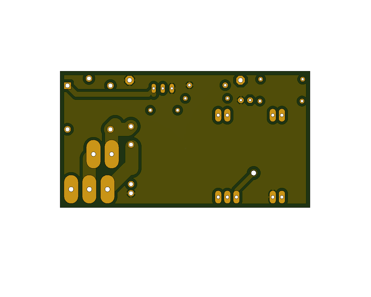
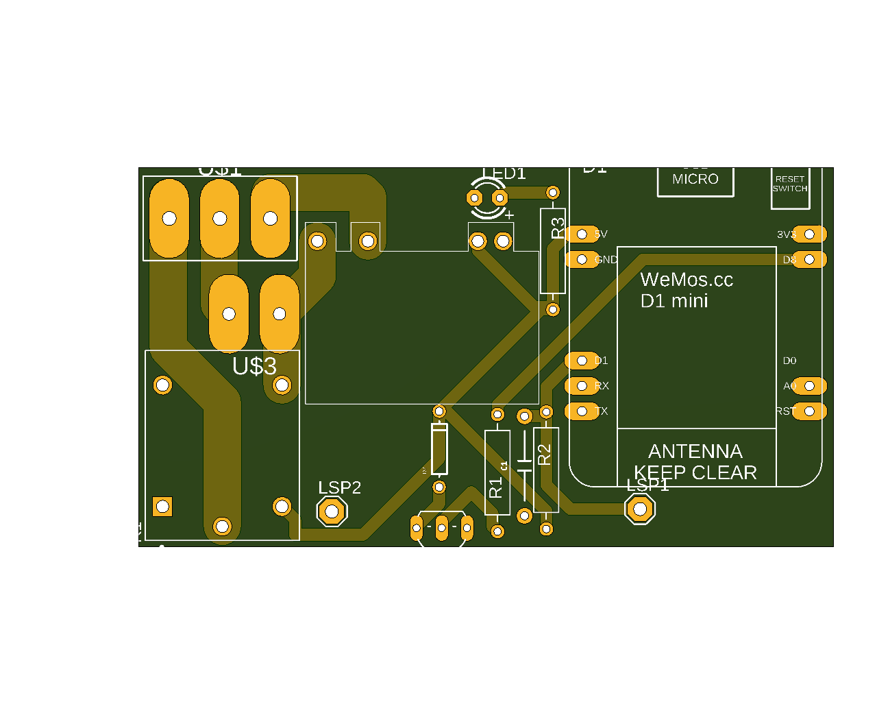
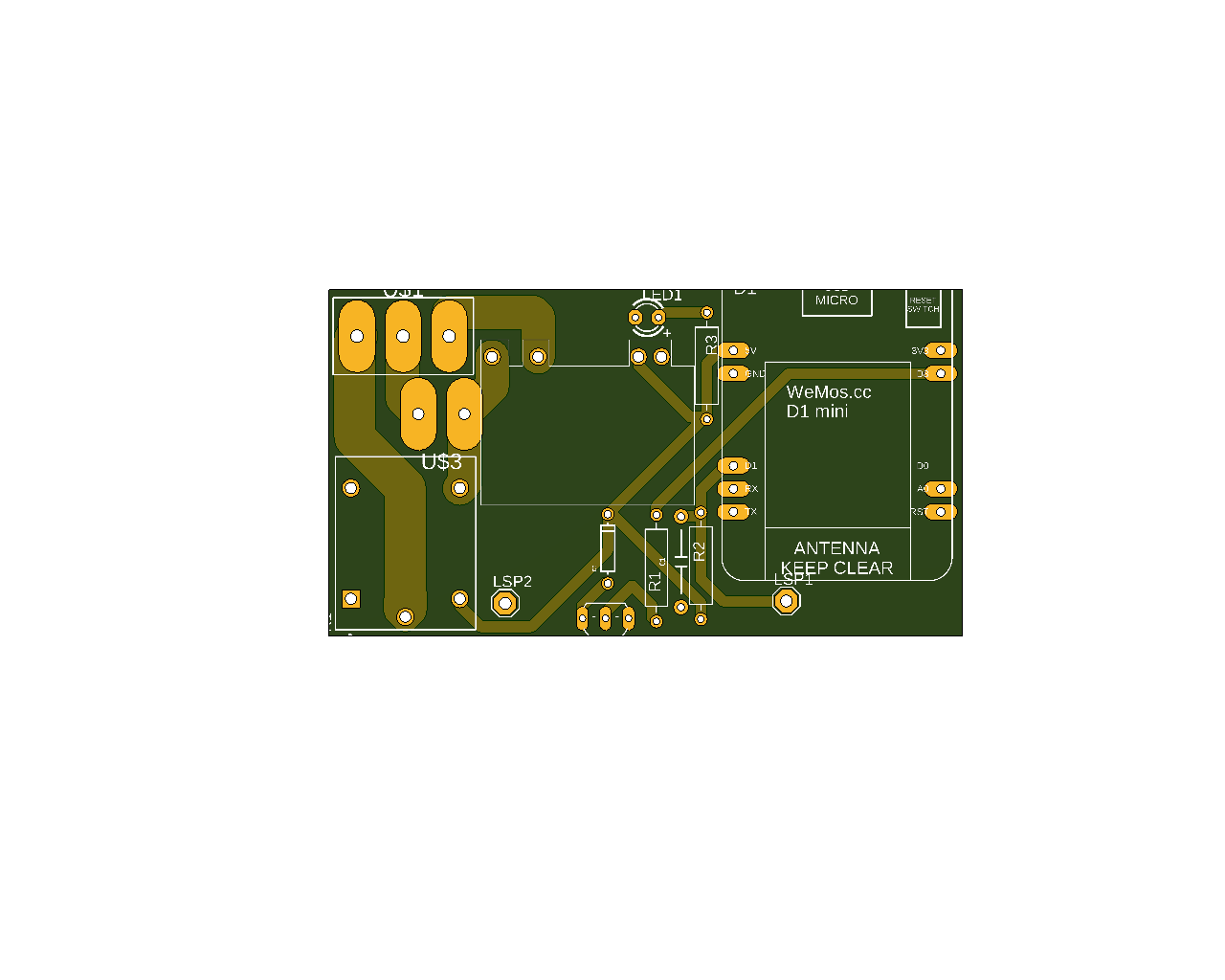
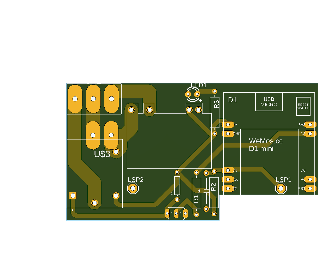
Here is my first take at it. I tried to do a better initial job than the last board you helped me with, but I don't know that I did. I made my high voltage traces as large as I could without getting too close to near by traces. I think all of the main voltage traces are .15 inches wide. Each of them are ran on the top of the board and the bottom of the board giving me about .3" trace width for the Mains voltage. I tried to keep them as short as possible for obvious reasons. I wasn't able to get a trace from the output of the relay (Pin that goes to the Load) to the screw terminal on top and bottom of the pcb all the way because the trace that goes from the transistor to the relay had to cross. This is the only place that the traces aren't doubled up completely for the main voltage lines. I placed the fuse as close to the screw terminal (where the incoming main voltage is coming in) as I could. As of now, I have .025 thermal width for the pads that are connecting to the ground pour. I also have a .028 gap for isolation between the ground pour and other traces. I am not sure if this enough or too much.
I did add a pullup resistor for the Input on D1, but I just now saw your recommendation for the capacitor for the switch debounce. I will go back and try to add it.
Ok.... Let me have it! I'm ready the corrections and criticism!
Working on adjustments! I will add led. Couple of questions. I read the article, but I'm not sure I understand where the cap goes to debounce the switch. There is an external pullup resistor. Does the cap attach to the pullup resistor and to ground? Does it matter which side of the resistor?
Does the pcb need physical cutouts in between the main traces and between the high/low voltage sides of the board to allow for heat dissipation or is the space I have good enough?
Working on adjustments! I will add led. Couple of questions. I read the article, but I'm not sure I understand where the cap goes to debounce the switch. There is an external pullup resistor. Does the cap attach to the pullup resistor and to ground? Does it matter which side of the resistor?
Capacitor goes across the switch.
Does the pcb need physical cutouts in between the main traces and between the high/low voltage sides of the board to allow for heat dissipation or is the space I have good enough?
AC traces are often isolated from logic traces with cutouts.
However, I have never done this, you decide what you want to do.
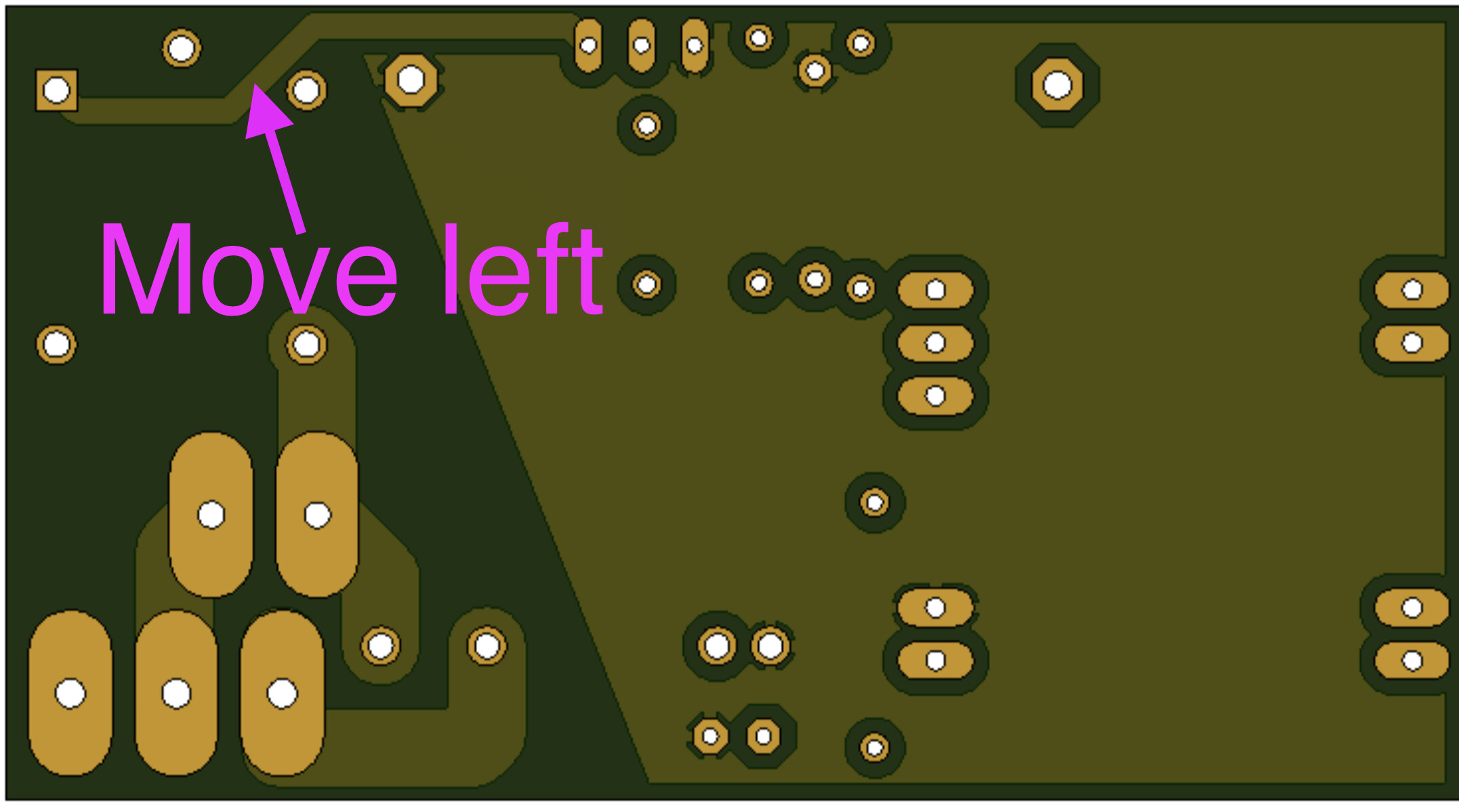
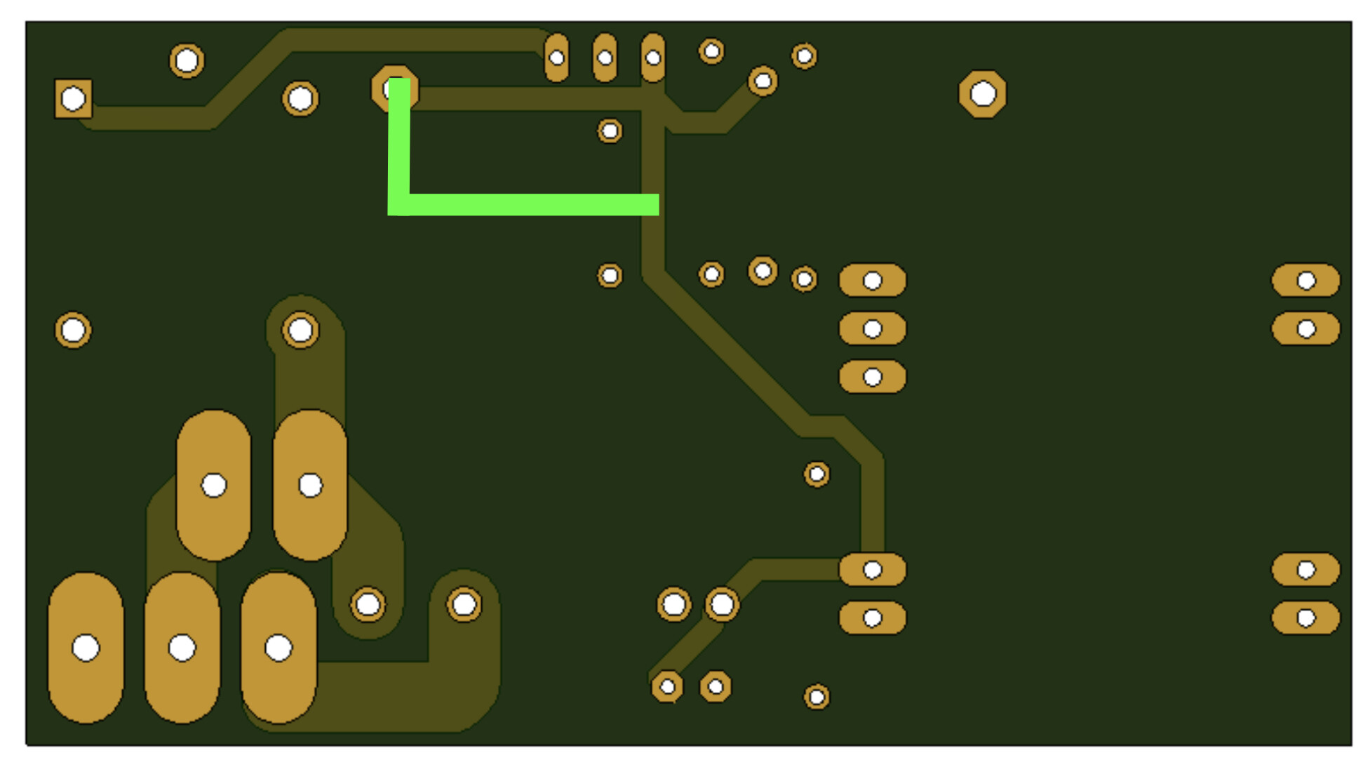
fat traces is mains. that pin is logic. Wayyy too close. Rotate that component 90° CW or something to keep the pcb spacing the same as the device pin spacing. By twisting it so the logic pins are adjacent to power, you violated the component's intrinsic isolation spacing.
Keep mains traces AT LEAST 1/2" away from ALL logic traces!
PS: normally you route horizontal runs on one side and vertical (cross overs) on the other. Sometimes you find you can go single sided with just a few crossing jumpers topside.
The coil wire to U$3 wanders towards the mains pins, NO! Go around, not BETWEEN. 1/2" creep MINIMUM
Draw a 1/2" wide line. All mains on one side, all logic on the other. The only things that cross that line are components, NO TRACES! The SHORTEST path should be the full component, no traces running closer than component leads. Thus, you have no arc over path other than the component limits.
Have you ever heard of a HIPOT tester? Google it. If your device cannot pass a 3kV HIPOT test, it is unsafe. That trace will ARC!
Don't flood the mains area to preserve isolation. You've only got 10 mills or so between the backside ground flood and the mains leads!
Ok, I made some changes to allow the low voltage side traces to stay at least as far away from the main voltage as their respective component. I have the logic traces set to .05" which I believe is rather large for logic traces and could be reduced if they appear to be to close to anything on the board, but someone once told be the copper was free on these boards so use it up. The main voltage traces are all .15" wide and ran on both sides of the board giving me .3" of trace width for all except the one trace that has to be crossed over by the coil trace of the relay.
I am considering removing the unused pad that is on the footprint of the relay so that I can make that trace (the one that I can't double the amount of copper by running it on top and bottom) wider. This would mean that pin on the relay would need to be removed before it could be soldered to the board.... I am not sure that would be acceptable.... But it was a thought I had.
I am also working on removing the vast majority of the ground pour that is near the mains wiring. It doesn't appear to be necessary to me.
I don't supposed I have to have the ground plane? I thought the large ground plane was supposed to prevent multiple long GND traces which pick up noise? The antenna placement is a concern I have received as well. I tried to keep the traces as far away as possible, but I don't really want the board physically hanging out over the pcb much if I don't have to. The antenna will actually be pointed away from the pcb I am designing not sandwiched in between. I am hopeful that this will allow a good radio signal, but I don't know.
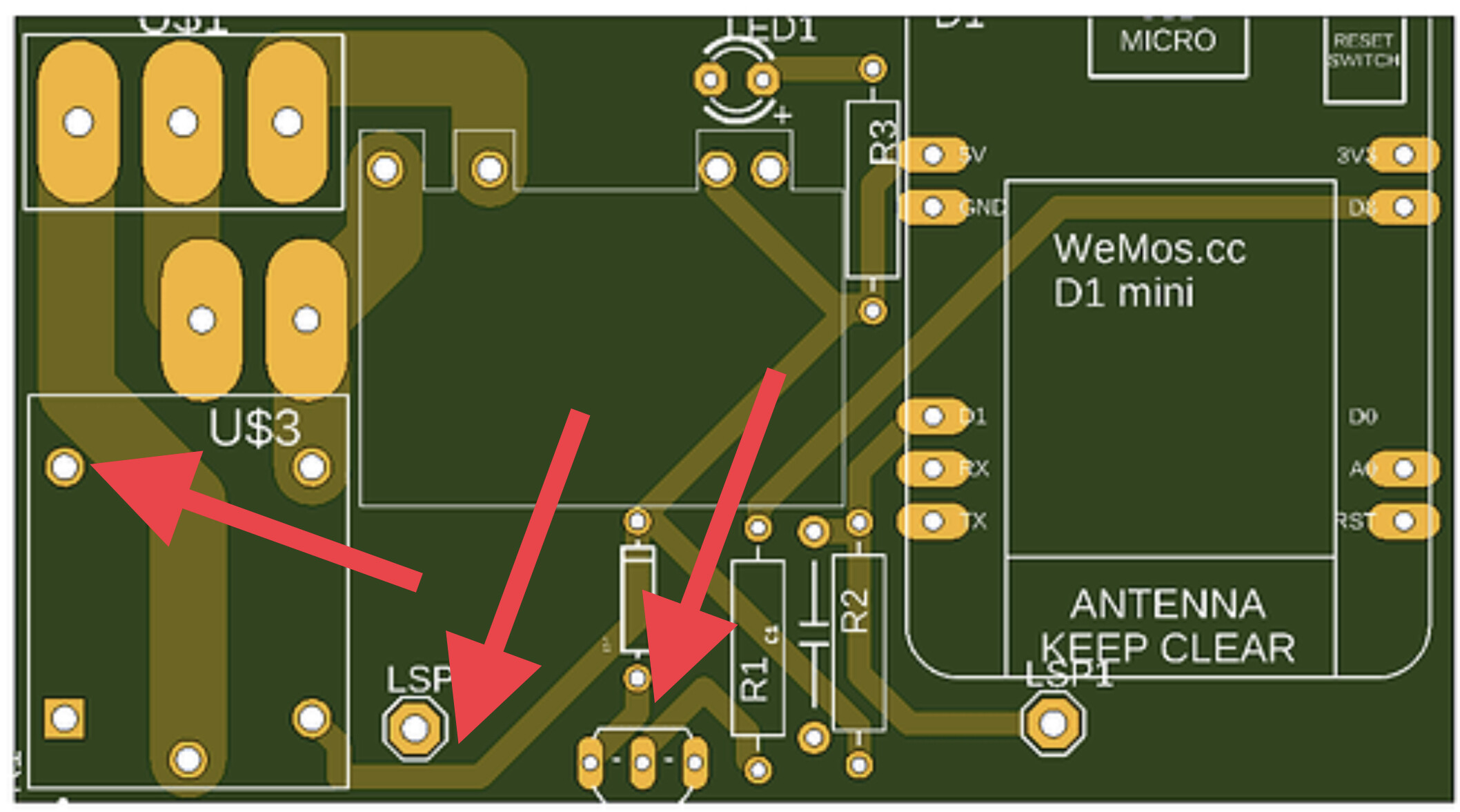
@LarryD I can definitely make the issue you pointed out to the farthest right better. No problem.
The middle arrow, I don't know what to do with. I can route it on the top side of the LSP2 connection point, but @madmark2150 is concerned with it being too close to the main voltage if the trace is closer to main voltage than the component itself. Honestly, I liked it above the LSP2 connection point, but obviously, I am no expert. The other options are making the traces smaller (it is .05" now) or having it go closer to the edge of the board. I am not sure how much clearance at the edge of the board is advisable?
The arrow on the far left is going near the pad that is not going to be used on the relay. This is the one that I contemplated taking out completely. This would allow me to make the trace larger for the one trace that I couldn't double up and run it on top and bottom. However, I would then have to physically clip one of the pins on the relay when I soldered to the board. I thought this may be frowned upon??
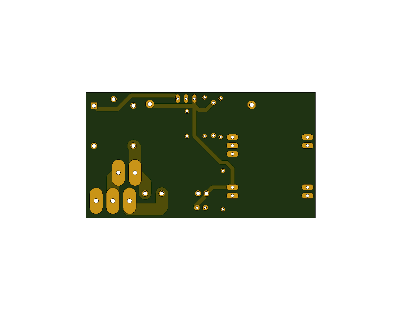
I was able to manipulate some components/traces and I think I have them a little better..... Still not sure whether to go under or over the LSP2 connection or make the traces smaller than .05"
I was actually able to make the Mains Voltage Load Trace that is only routed on the top wider (from .15" to .18") and increase the clearance between the relay pad that you pointed out with your far left arrow.
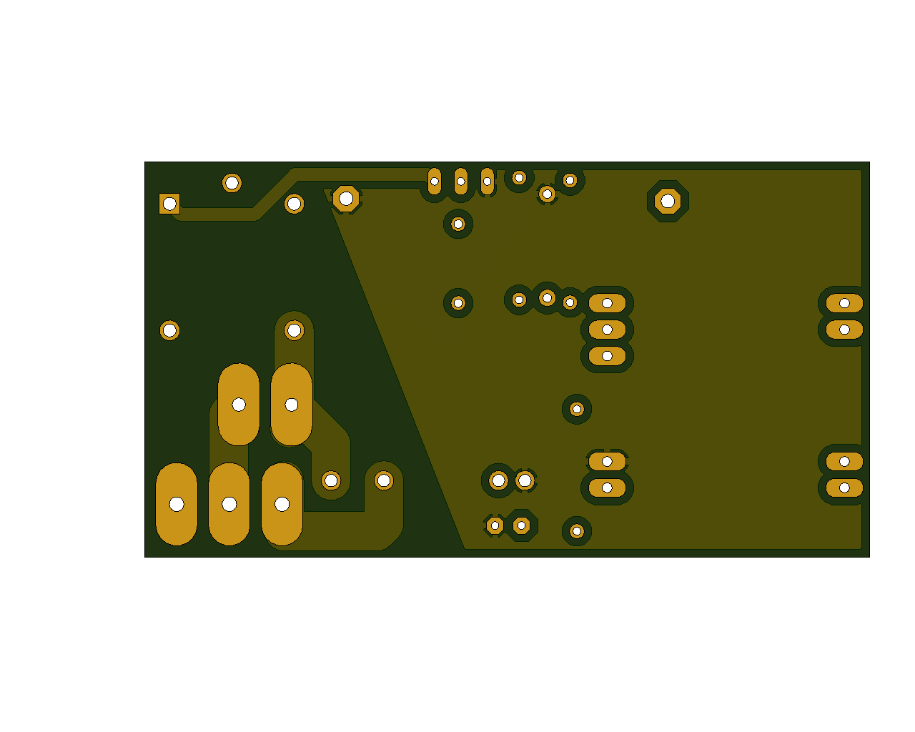
I left the ground plane on bottom for now. I am looking to see how many long ground traces would be needed to eliminate the ground plane.
Ok, I noticed that while I was making changes from ground plane to ground traces. here it is with ground the ground plane removed and ground using ground traces. Which one looks better?
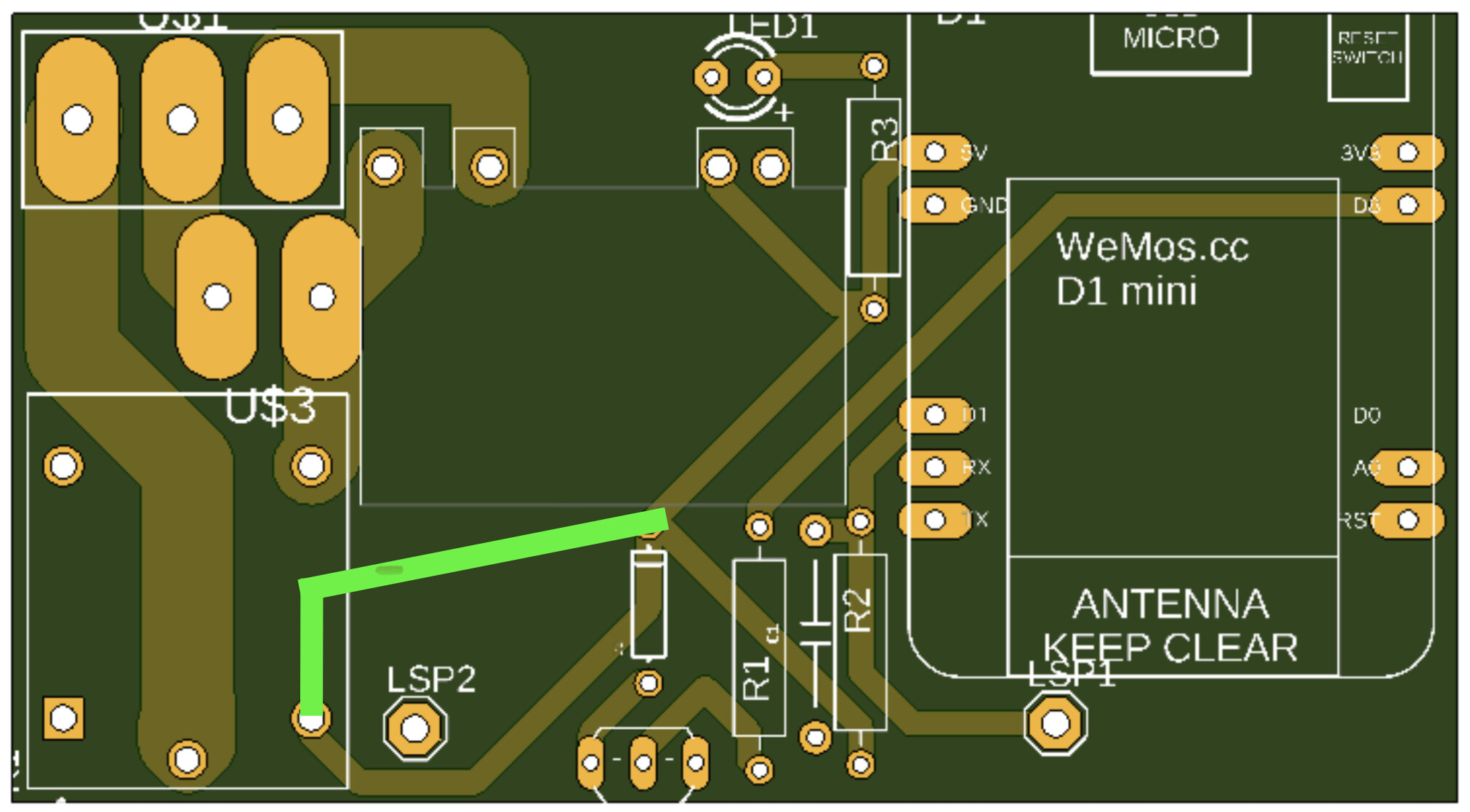
So, I've made some more adjustments to the pcb. I was able to find some power relays with similar footprints to the songle relay, and they are from a reputable site! I contemplated trimming one of the pins from the relay to allow more room for the trace that goes from the common pin of relay to the load output screw terminal. However, I was able to find that some relays eliminate this pin for you (has no NC pin)! This allows me to be able to run ALL of the MAIN voltage traces doubled up on top and bottom (.3+" of copper total).
Here is just one link to a relay I am talking about. There are several that will work that I have found.
There was also a concern about the antenna on the wemos D1 mini being covered by the pcb and hindering its radio signal capabilities. I adjusted the pcb so that I could remove part of my pcb to prevent blocking the antenna portion of the wemos board.
Here are some pics of it now, let me know what y'all think!