I have an UNO R3 pins D18 and D19 are the SDA and SCL pins respectively. I have connected them to a camera Ov7670, yes with pull up resistors (4.7k) to VCC. GND and 3V3 both connected. First i tried on A4 and A5 i thought maybe the wires are too long and noisy so i swithed to the other side labelled SCL and SDA. (Speaking of which why do projects use A4 A5?) Still in either case for all 127 addresses it returns errror 2, address byte NACK. For code i used the i2c scanner example sketch. Then i modified it to also print the number of occurances of each error type.
I quadruple checked the wiring, it is according to schematics. What else could be the problem? i dont really have multimeters or other measurement tools but i could use an LED to probe- sigh...
You only need one. They are inexpensive and easily available. Get one. They are so useful!
On Uno R3, A4 & A5 are the i2c pins because Uno has an ATmega328 chip, and on that chip, they are dual function. They can be used as either A4 & A5 analog inputs, or they can be used as SCL & SDA i2c pins. But not both at the same time.

On other Arduino boards which use other chips, things will be different. Look at Leonardo, for example. That uses an ATmega32u4 chip. On that chip, the i2c pins are completely different.
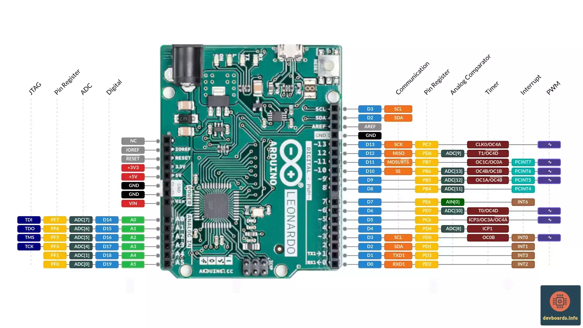
But both Uno R3 and Leonardo can share the same shields, at least for the ones that use i2c. It works because those 2 pins, at the top-right of the board, are always i2c regardless of the chip used.
If you hand-draw your actual wiring, take a photo of the drawing and post it as a reply to this, I will replicate it here with my UNO and tell you the results.
I will also run my I2C scanner and post results.
On the UNO R3, the A4 pin is directly connected to the SDA pin via a circuit board trace, likewise for A5 and SCL. That was done for "convenience" but seems to create more confusion for beginners.
I'm retracting this... i saw the light...
There are only two ends of two wires to check. Verify SDA goes to A4 (because DATA has four letters) and CLK goes to A5 (because CLOCK has five letters) and run the Arduino I2C bus scan.

What is VCC?
Do you mean 3.3V?
- Making friends and influencing others are you
 ?
?
Thissiteisstupid
-
The camera is 3v3, UNO is 5v, where is your signal level shifting ?
-
Always show us a good schematic of your proposed circuit. Show us good images of your ‘actual’ wiring. Give links to components.
-
In the Arduino IDE, use Ctrl T or CMD T to format your code then copy the complete sketch. Use the < CODE / > icon from the ‘posting menu’ to attach the copied sketch.
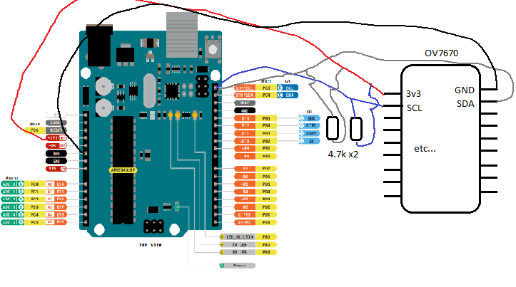
As per ypur request "hand drawn" in Paint, not sponsored
Edit: double checked with https://resistorcolorcodecalc.com
I used 10k haha
yes i'm familiar with circuit digest, thank you. I have already referenced the schematic you're showing
i mean yeah i understand that they're connected, my question was more of a "why use one of the few pins that can take analog signals when you have to other pins specifically labelled scl and sda"
The camera is 3v3, UNO is 5v
okay i've heard that before but it has those little 3V3 pins is that no good? ![]() i can't just use the 3v3 to power the 3v3 cam?
i can't just use the 3v3 to power the 3v3 cam?
a good schematic
Ah yes a good shematic, a shematic that is good that which i most certaily posess, that schematic ![]() When you say give links to components do you mean their documentation? i have an ov7670 doc but it's for the omnivision camerachip i think and the pinout of the camera module is more limited with only 18-ish pins, i don't have docs for that specifically. and as i've said i used a built in sketch provided in the examples.. then i modified what it shows on the serial monitor so here is my version it shows Adress NACK for all 127 addresses we're checking
When you say give links to components do you mean their documentation? i have an ov7670 doc but it's for the omnivision camerachip i think and the pinout of the camera module is more limited with only 18-ish pins, i don't have docs for that specifically. and as i've said i used a built in sketch provided in the examples.. then i modified what it shows on the serial monitor so here is my version it shows Adress NACK for all 127 addresses we're checking
// --------------------------------------
// i2c_scanner
//
// Version 1
//    This program (or code that looks like it)
//    can be found in many places.
//    For example on the Arduino.cc forum.
//    The original author is not known.
// Version 2, Juni 2012, Using Arduino 1.0.1
//     Adapted to be as simple as possible by Arduino.cc user Krodal
// Version 3, Feb 26  2013
//    V3 by louarnold
// Version 4, March 3, 2013, Using Arduino 1.0.3
//    by Arduino.cc user Krodal.
//    Changes by louarnold removed.
//    Scanning addresses changed from 0...127 to 1...119,
//    according to the i2c scanner by Nick Gammon
//    https://www.gammon.com.au/forum/?id=10896
// Version 5, March 28, 2013
//    As version 4, but address scans now to 127.
//    A sensor seems to use address 120.
// Version 6, November 27, 2015.
//    Added waiting for the Leonardo serial communication.
//
//
// This sketch tests the standard 7-bit addresses
// Devices with higher bit address might not be seen properly.
//

#include <Wire.h>

void setup() {
  Wire.begin();

  Serial.begin(9600);
  while (!Serial)
    ;  // Leonardo: wait for Serial Monitor
  Serial.println("\nI2C Scanner");
}

void loop() {
  int nDevices = 0;
  int error1 = 0;
  int error2 = 0;
  int error3 = 0;
  int error4 = 0;
  int error5 = 0;
  Serial.println("Scanning...");

  for (byte address = 0; address < 127; ++address) {
    // The i2c_scanner uses the return value of
    // the Wire.endTransmission to see if
    // a device did acknowledge to the address.
    Wire.beginTransmission(address);
    byte error = Wire.endTransmission();
    if (error == 0) {
      Serial.print("Device found at 0x");
      if (address < 16)
        Serial.print("0");
      Serial.print(address, HEX);
    }
    if (error == 1) error1++;
    if (error == 2) error2++;
    if (error == 3) error3++;
    if (error == 4) error4++;
    if (error == 5) error5++;
  }
  Serial.println("Number of errors:");
  Serial.print("Address byte NACK:");
  Serial.println(error2);
  Serial.print("Other errorbyte NACK:");
  Serial.println(error4);
  Serial.print("Data byte NACK:");
  Serial.println(error3);
  Serial.print("Data exceeds buffer capacity:");
  Serial.println(error1);
  Serial.print("Time-out:");
  Serial.println(error5);
  delay(5000);  // Wait 5 seconds for next scan
}
I don't see the level shifter for SDA/SCL
It's NOT for powering the cam, it's the SCL/SDA pins. The UNO I2C pins will be 5V and you are connecting them to a 3.3V board. POOF, magic smoke.
Seems the designer of the tutorial didn't bother with level shifters...
I have just been looking at the Datasheet for the OV7670 and am wondering whether this can actually work. The IO voltage range is between 1.7V and 3.0V. The output voltage is stated as 0.9 of VDD, so at 3.0 this would be 2.7V. Even at 3.3V (as its being driven from a 3.3V regulator) this would be 2.97V. I2C requires between 0.6 and 0.7 of VDD for a logic high level which on a 5V UNO would be between 3.0V and 3.5V which seems very marginal at best.
Furthermore, the IO voltage tolerance is stated as "-0.3V to VDD-IO+0.5V", so a max of 3.5V would seem to apply. Level shifters would certainly be needed to interface with a 5V board safely.
https://web.mit.edu/6.111/www/f2016/tools/OV7670_2006.pdf
OP might be better off just using a 3.3V board.
If my reading of the datasheet is incorrect then by all means let me know.
oh shi-
i have read what you mentioned somewhere else before but i was only thinking about powering the cam corretly
this did not occur to me at all as a possibility
Is my camer caput? i guess if i do this magical level shifting i'll find out
so what about this that was shared in a comment by xfpd
that's basically what i got as well just rn connected to SCL and SDA but it's the same thing
He retracted it. You just need to insert a level shifter between the UNO SCL and SDA pins and the wire going to the camera.
You can make sense of the data sheet? All those mysterious VDD stuff mean something to you? How do i learn that? I'm studying related things in university and it did not help at all. And I'm not one of those who party and skip classes. The future is bleak.
+Questions:
- why is the logical high between 3 and 3.5 if the somethingelse is 5V
- if the highest voltage that vcan come from the UNO 3.5 and the cam tolerance has a max of 3.5 what is the problem? sounds like the magic smoke wont leave my camera
Is it perhaps that the cam cannot send back a igh enough voltage for it to register as a high logic? but the line is pulled up to 3v3...
Is it the logical lows that we're having trouble with then?
it's so confusing
how the hell am i supposed to make sense of all this all on my own
how do people learn this shi
I beg to differ if you are careful. I2C is open drain, the voltage on the pins depends on the pull up resistors, so if pull up is to 3V3 then there won't be any damage. You might get away with pull up to 5V because the resistors will limit the current, which will flow into the input protection diodes of the 3V3 device, limiting the voltage to what the device can tolerate. However, relying on protection diodes in this way, while it might work, is terrible practice. The remaining risk is setting the pins of the 5V device to output then high, that very well might kill the 3V3 device.
In summary for @thissiteisstupid if you have connected I2C between a 3V3 device and a 5V device and pulled up to 3V3 then there's a good chance you have not killed anything. Whether it will work without level shifters is a different matter, it might but don't count on it. If it works, good. If it doesn't work then fix the obvious problem first: get level shifters. Make sure they are suitable for I2C (not all are).
- You mean the wiring and schematic you refuse to show us ?
![]()