That means the information supplied by ChatGPT is post #12 is inaccurate/fake. The GPIO2/GPIO23 of the sketch of post #1 belongs to Core 1 (by default).
Do you have any idea or sketch by which the said digital pins can be connected/directed to Core 0 and let the LEDs be blinking?
I'm lost - what don't you understand in this statement:
the GPIO (General Purpose Input/Output) pins on the ESP32 microcontroller are not tied to specific cores. Both Core 0 and Core 1 have access to and can control all the GPIO pins available on the ESP32
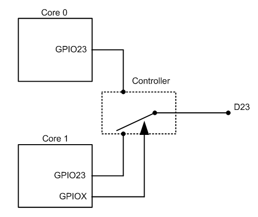
If the IO pins/lines of the ESP32S are not permanently tied to (default to Core 1?) any core, then there should be a software controlled switch/controller (Fig-1: installed by Espressif) that directs the IO line(s) either to Core 0 or Core 1 as requested -- is it correct?
Figure-1:
D23 is an IO line on the header of ESP32S Module. There are two independent LX6 processors mounted (under the RF Shield) on the ESP32S Breakout Board/Module with their own GPIO23 IO line. The D23 line of the Module can be routed to the GPIO23 line either of Core 0 or Core 1. How is it possible to have this kind of changeover without a hardware switch conceptually similar to Fig-1 of post #32?
If you are talking about accessing the external common Flash Memory, then there must be (in association with controlling software) an external SPI Controller to route the SPI lines either of Core 0 or Core 1 to the IO lines of the Flash Memory (Fig-1).
Figure-1:
that's where you got confused. The Tensilica Xtensa 32-bit LX6 microprocessor has two cores embedded in one chip. it's not two separate microprocessors
Then the cores have intercommunication mechanism and all the necessary hardware to route the IO lines of the header pins of the ESP32S Module or of the external flash memory either to Core 0 or Core 1.
Referring to the block diagram of your post #3, it can be said that the ESP32S Board is composed of two CPU/MPU units/cores (having their ALU Unit, Register Set, and Sequence generator) and single unit of other hardware resources.
There are no two sets of IO lines as I thought before and all the confusions raised from there, which you have correctly pin-pointed and have successfully got me out of the trap.
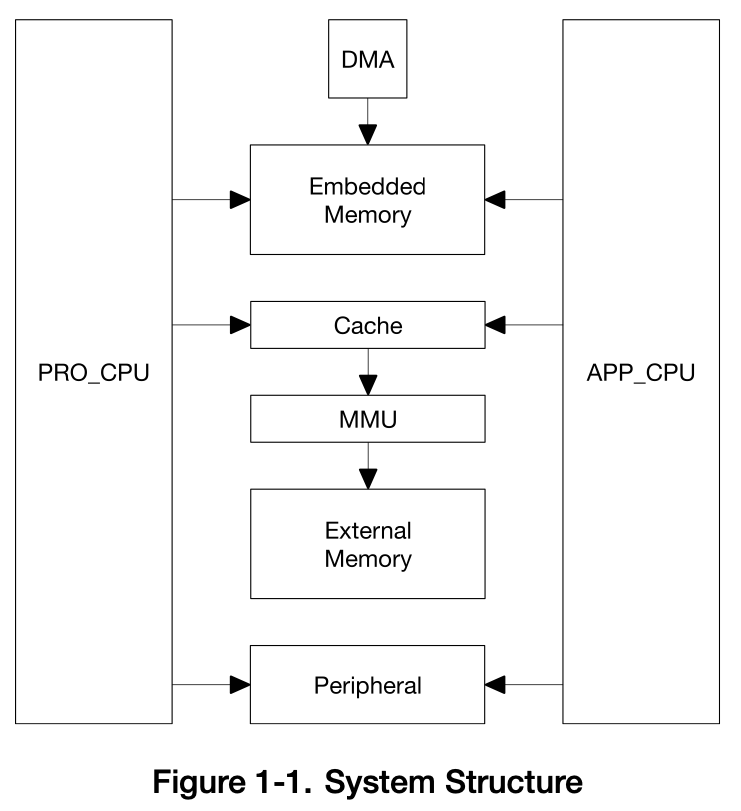
The ESP32 is a dual-core system with two Harvard Architecture core. All embedded memory, external memory and peripherals are located on the data bus and/or the instruction bus of these CPUs.
The two cores are known as the PRO(tocol) Core and the APP(lication) core (pr "PRO_CPU” and “APP_CPU” and the two cores are interchangeable.
The address mapping of two cores is symmetric, meaning that they use the same addresses to access the same memory (one exception is the PID Controller). Multiple peripherals in the system can access embedded memory via DMA.
Each core can directly access embedded memory through both the data bus and the instruction bus, external memory which is mapped into the address space via transparent caching & MMU, and peripherals.
The address mapping, GPIOs are one of the 41 peripherals.
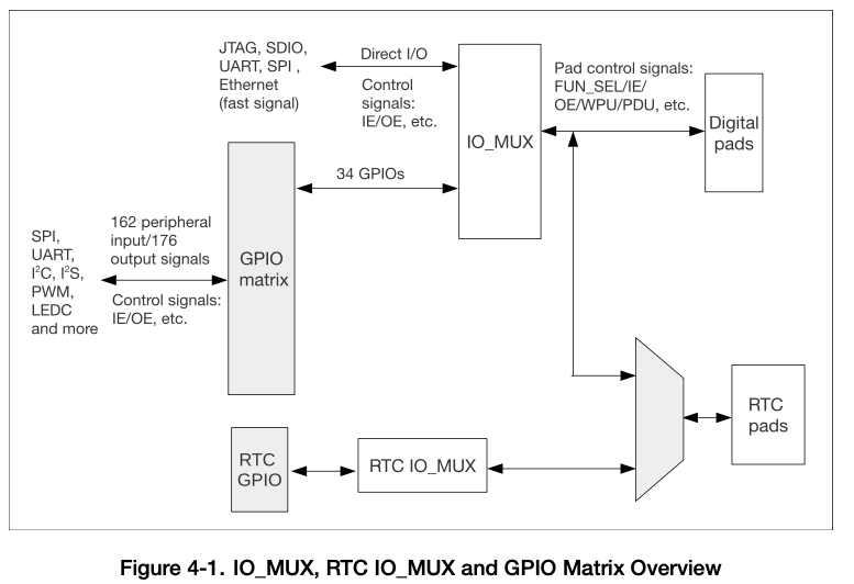
The ESP32 chip features 34 physical GPIO pads. Each pad can be used as a general-purpose I/O, or be connected to an internal peripheral signal. The IO_MUX, RTC IO_MUX and the GPIO matrix are responsible for routing signals from the peripherals to GPIO pads. 1. The GPIO Matrix is a full-switching matrix between the peripheral input/output signals and the pads
I have tested your sketch and it is working in the sense that the LEDs are blinking as intended.
Few more questions/queries will be inline once I finish reading/understanding the newly arrived code lines/syntaxes of your sketch like xCreatePinnedToCore.
However, I am convinced that LED2 is being driven by Core 0 as it it outside of the loop() function and I need to verify it probably by reading the ChipIDs.