westfw:
Look at the ...**/packages/**vendor/**hardware/nrf52/*version/variants/boardname file.
In that directory, there should be a file that contains the mapping from pin numbers to chip-specific ports and bits and such (usually "variant.h", "variant.cpp", or "pins_arduino."
I've already checked variant.h and variant.cpp which are located at **\packages\sandeepmistry\hardware\nRF5\0.6.0\variants\Generic**.
Still not clear for me how digital pins are assigned to IDE pin numbers:
variant.cpp
#include "variant.h"

const uint32_t g_ADigitalPinMap[] = {
  0,
  1,
  2,
  3,
  4,
  5,
  6,
  7,
  8,
  9,
  10,
  11,
  12,
  13,
  14,
  15,
  16,
  17,
  18,
  19,
  20,
  21,
  22,
  23,
  24,
  25,
  26,
  27,
  28,
  29,
  30,
  31
};
variant.h
#ifndef _VARIANT_GENERIC_
#define _VARIANT_GENERIC_

/** Master clock frequency */
#ifdef NRF52
#define VARIANT_MCK       (64000000ul)
#else
#define VARIANT_MCK       (16000000ul)
#endif

/*----------------------------------------------------------------------------
 *        Headers
 *----------------------------------------------------------------------------*/

#include "WVariant.h"

#ifdef __cplusplus
extern "C"
{
#endif // __cplusplus

// Number of pins defined in PinDescription array
#define PINS_COUNT           (32u)
#define NUM_DIGITAL_PINS     (32u)
#define NUM_ANALOG_INPUTS    (6u)
#define NUM_ANALOG_OUTPUTS   (0u)

// LEDs
#define PIN_LED              (13) // P0.13
#define LED_BUILTIN          PIN_LED

/*
 * Analog pins
 */
#define PIN_A0               (1) // P0.01
#define PIN_A1               (2) // P0.02
#define PIN_A2               (3) // P0.03
#define PIN_A3               (4) // P0.04
#define PIN_A4               (5) // P0.05
#define PIN_A5               (6) // P0.06

static const uint8_t A0  = PIN_A0 ;
static const uint8_t A1  = PIN_A1 ;
static const uint8_t A2  = PIN_A2 ;
static const uint8_t A3  = PIN_A3 ;
static const uint8_t A4  = PIN_A4 ;
static const uint8_t A5  = PIN_A5 ;
#ifdef NRF52
#define ADC_RESOLUTION    14
#else
#define ADC_RESOLUTION    10
#endif

/*
 * Serial interfaces
 */
// Serial
#define PIN_SERIAL_RX       (0) // P0.00
#define PIN_SERIAL_TX       (1) // P0.01

/*
 * SPI Interfaces
 */
#define SPI_INTERFACES_COUNT 1

#define PIN_SPI_MISO         (22) // P0.22
#define PIN_SPI_MOSI         (23) // P0.23
#define PIN_SPI_SCK          (24) // P0.24

static const uint8_t SS   = 25 ;  // P0.25
static const uint8_t MOSI = PIN_SPI_MOSI ;
static const uint8_t MISO = PIN_SPI_MISO ;
static const uint8_t SCK  = PIN_SPI_SCK ;

/*
 * Wire Interfaces
 */
#define WIRE_INTERFACES_COUNT 1

#define PIN_WIRE_SDA         (20u) // P0.20
#define PIN_WIRE_SCL         (21u) // P0.21

static const uint8_t SDA = PIN_WIRE_SDA;
static const uint8_t SCL = PIN_WIRE_SCL;

#ifdef __cplusplus
}
#endif

#endif
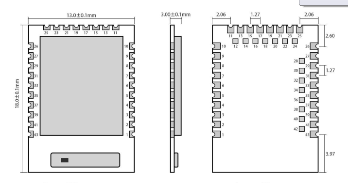
Here is my board:


I like how it's done for Feather nRF52840 board:
#include "variant.h"
#include "wiring_constants.h"
#include "wiring_digital.h"
#include "nrf.h"

const uint32_t g_ADigitalPinMap[] =
{
  // D0 .. D13
  25,  // D0  is P0.25 (UART TX)
  24,  // D1  is P0.24 (UART RX
  10,  // D2  is P0.10 (NFC2)
  47,  // D3  is P1.15 (LED1)
  42,  // D4  is P1.10 (LED2)
  40,  // D5  is P1.08
   7,  // D6  is P0.07
  34,  // D7  is P1.02 (Button)
  16,  // D8  is P0.16 (NeoPixel)
  26,  // D9  is P0.26
  27,  // D10 is P0.27
   6,  // D11 is P0.06
   8,  // D12 is P0.08
  41,  // D13 is P1.09

  // D14 .. D21 (aka A0 .. A7)
   4,  // D14 is P0.04 (A0)
   5,  // D15 is P0.05 (A1)
  30,  // D16 is P0.30 (A2)
  28,  // D17 is P0.28 (A3)
   2,  // D18 is P0.02 (A4)
   3,  // D19 is P0.03 (A5)
  29,  // D20 is P0.29 (A6, Battery)
  31,  // D21 is P0.31 (A7, ARef)

  // D22 .. D23 (aka I2C pins)
  12,  // D22 is P0.12 (SDA)
  11,  // D23 is P0.11 (SCL)

  // D24 .. D26 (aka SPI pins)
  15,  // D24 is P0.15 (SPI MISO)
  13,  // D25 is P0.13 (SPI MOSI)
  14,  // D26 is P0.14 (SPI SCK )

  // QSPI pins (not exposed via any header / test point)
  19,  // D27 is P0.19 (QSPI CLK)
  20,  // D28 is P0.20 (QSPI CS)
  17,  // D29 is P0.17 (QSPI Data 0)
  22,  // D30 is P0.22 (QSPI Data 1)
  23,  // D31 is P0.23 (QSPI Data 2)
  21,  // D32 is P0.21 (QSPI Data 3)

  // The remaining NFC pin
   9,  // D33 is P0.09 (NFC1, exposed only via test point on bottom of board)

  // Thus, there are 34 defined pins

  // The remaining pins are not usable:
  //
  //
  // The following pins were never listed as they were considered unusable
  //  0,      // P0.00 is XL1   (attached to 32.768kHz crystal)
  //  1,      // P0.01 is XL2   (attached to 32.768kHz crystal)
  // 18,      // P0.18 is RESET (attached to switch)
  // 32,      // P1.00 is SWO   (attached to debug header)
  //
  // The remaining pins are not connected (per schematic)
  // 33,      // P1.01 is not connected per schematic
  // 35,      // P1.03 is not connected per schematic
  // 36,      // P1.04 is not connected per schematic
  // 37,      // P1.05 is not connected per schematic
  // 38,      // P1.06 is not connected per schematic
  // 39,      // P1.07 is not connected per schematic
  // 43,      // P1.11 is not connected per schematic
  // 44,      // P1.12 is not connected per schematic
  // 45,      // P1.13 is not connected per schematic
  // 46,      // P1.14 is not connected per schematic
};