I2C decoding (DS3231)

Hello, I was curious about I2C bus low level signals, so I checked a communication sequence of reading status register (address 0x0F) and time registers of a DS3231 (DS3231RTC library) RTC. But there are a few things which I don't understand.

1.

uint8_t statusReg = 255;
RTC.readRTC(0x0F, &statusReg, 1);

Result:


Start bit, address, R/W, ACK. But what is the pulse marked with question marks?

2.

RTC.read(DateTime);

This starts a 7 byte read through the library, starting with 0x00 address (RTC_SECONDS).
Result:


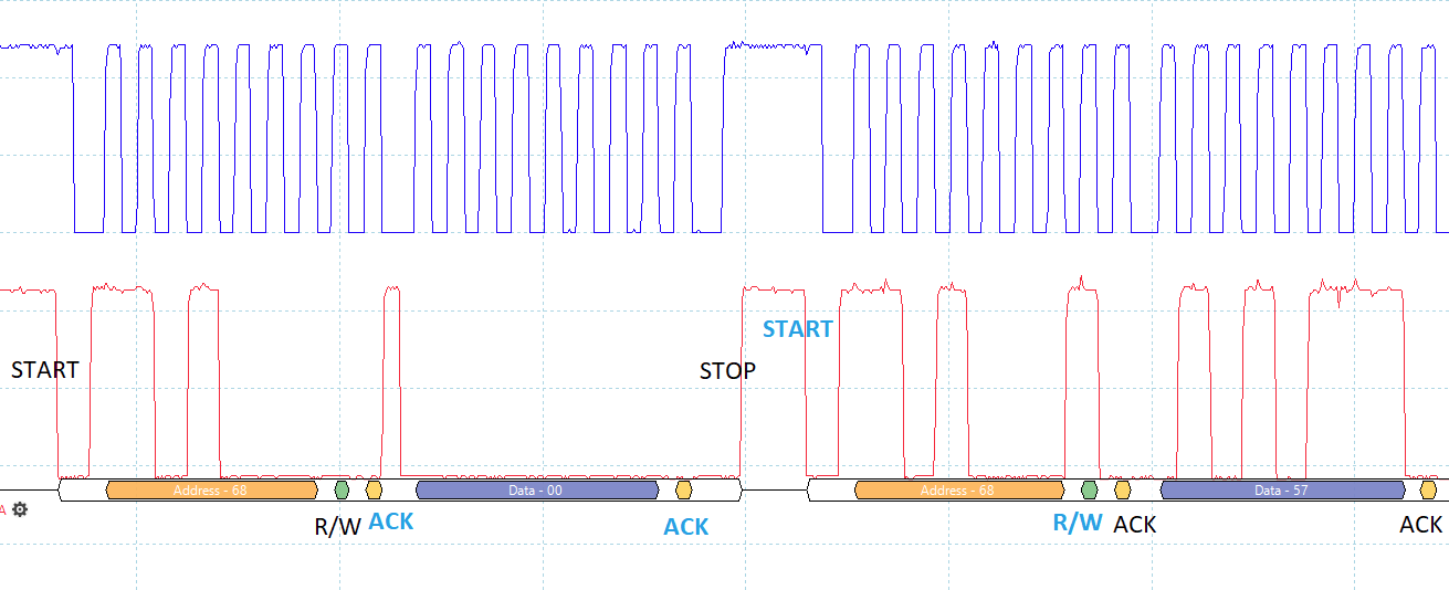
First address was sent like in the first point. My question is that the second START is initated by the RTC module itself, right? So roles change, and after the second start, the ACK is coming from the uC?

3.
This is about twi.c. I found where the R/W bit is controlled for example for read:

  // build sla+w, slave device address + w bit
  twi_slarw = TW_READ;
  twi_slarw |= address << 1;

And I understand that the blocking read/send is controlled through twi_state. For read:


  // wait until twi is ready, become master receiver
  uint32_t startMicros = micros();
  while(TWI_READY != twi_state){
    if((twi_timeout_us > 0ul) && ((micros() - startMicros) > twi_timeout_us)) {
      twi_handleTimeout(twi_do_reset_on_timeout);
      return 0;
    }
  }

And this leads to the interrupt vector for TWI where twi_status is altered and could became TWI_READY to exit the upper while cycle.

ISR(TWI_vect)
{
  switch(TW_STATUS){
  .
  .
  .

But what is this TW_STATUS and the switch cases values? TW_STATUS is already the TWI status register? I couldn't find a define or any clue for it.

Thanks in advance.

Those are what you called "REPEATED START". On your first diagram, you are reading a register but before you read the register, you must tell the DS3231 which register to read. Hence, you have a "write" register in your first transaction, but instead of "STOPPING" the transaction after the byte was written, the bus master issued a "repeated start", and proceeded with reading....

The second transaction didn't use a repeated start. It "STOPPED" the transaction and started a new one instead of combining the "STOP and START" into a "REPEATED START"

I think that the slave (receiver) releases SDA after ACK before the master pulls it low again.

Everything in $Arduino\hardware\tools\avr\avr\include\util\twi.h
#define TW_STATUS (TWSR & TW_STATUS_MASK)

First I thought of a repeated start also, but the SCL line should be high at the falling edge of that pulse in case of a repeated start. So I think @DrDiettrich is right. This diagram show a pulse like that also, but it's not labelled at all.

@DrDiettrich: Thanks, I found it!
My mistake, I only looked in this header.
C:\Program Files (x86)\Arduino\hardware\arduino\avr\libraries\Wire\src\utility\twi.h

I had the same problem, that's why I posted the long path.

Which equipment do you use ?
A USB Logic Analyzer of 10 or 30 dollars together with sigrok/PulseView is a great tool. PulseView has many decoders, also a I2C decoder. Then it will show the START, STOP, ACK and data for you. I'm very fond of the LHT00SU1 Logic Analyzer.

It's the PicoScope softwares standard I2C serial decoding function. Everthing is shown correctly, just the snapshots are zoomed out so R/W (green thing) and ACK (yellow) text is not visible.

Ok, I think 1. and 3. question has a solution. I think 2. question was asked incorrectly.

I edited the snapshot again and color coded SDA sections where I think the bit(s)/pull-down came from in that particular part. Are the markings for data/ACK bits are correct? Thanks in advance.

The first two bytes come from the µC and indicate the slave address and register number.The following bytes are a read cycle where the µC master again provides the slave address and read request whereupon the slave sends the following bytes until the µC stops the transmission.

For 3. you also should look into Wire.c how the low level twi functions are called.

I'm sorry, but I don't understand the question.
PulseView shows all the START, STOP, ACK, NACK, and so on. So you don't have to add labels or color it or check the pulses to see what is what.

@DrDiettrich: That's right, I started line-by-line reading in Wire.c and lower twi.c, but I wasn't quite persistent. But for the second run, I think I got the whole package.

..whereupon the slave sends the following bytes until the µC stops the transmission.

I figured out this part also (shame I didn't take any snapshot). To be accurate, the uC NACK response stops the RTC sending more than 7 bytes in this case (BCD 57 was the first on the right side of the picture). And the STOP condition comes after NACK.

@Koepel: The later question was not about recognizing the conditions and bits anymore . I was trying to figure out where did the actual Address / R/W / ACK / Data bytes and bits came from (who pulled down SDA line and when).

Think in 1980's hardware logic. That is how old the I2C bus is.

The Master is always in control. It sends the START, the I2C address, the R/W bit, the STOP, it gives the SCL clock.
When sending or receiving data, the ACK after a databyte tells the other side to latch new data in the shift-register and the SCL is the clock pulse for that shift-register.

When the Master is sending data, then the Slave gives an ACK to its I2C address and a ACK after each databyte when receiving data.
When the Master is requesting data, the Master gives that ACK after each databyte. That ACK is not needed for the last databyte, so the Master omits that one and just gives a STOP.

Sometimes you will see glitches. That does not violate the I2C standard, but it is not nice. Extra pulses could cause extra noise.

If we look into the register level codes, we observe that the ACK signal (indicating the end of current TWI Bus cycle) helps to produce bus status signal which the MCU/program uses to take next action.

SCL pulses are automatically generaed when a data byte is written into the TWDR Register like the genration of SCK pulses when a data byte is written into the SPDR Register.

No. The clock pulses, NACK and Stop are exclusively generated by the master/receiver, the slave/sender cannot terminate the transmission.

The master has exclusive control of SDA while SCL is high. In this state SDA transitions signal Start and Stop conditions. The transmitted information is sampled at the SCL falling edge. A slave only can extend the SCL low state (clock stretching).

Thanks for the info. It all makes sense now, and the ACK "source" is also logical in different data flow directions.

When the Master is requesting data, the Master gives that ACK after each databyte. That ACK is not needed for the last databyte, so the Master omits that one and just gives a STOP.

I think it is not omitted, at least with this ATmega2560-DS3231 setup. I hooked up the setup again and this is the 7 bytes transfer from the RTC after the uC request.

After the last, (BCD)22 byte, there is a ACK HIGH (NACK) and then the STOP condition (blue SCL high, red SDA rising edge)

No. The clock pulses, NACK and Stop are exclusively generated by the master/receiver, the slave/sender cannot terminate the transmission.

That's what the sentence (which you quoted) meaning intended to be, sorry if it was not clear enough. The master indicated with NACK that the slave should not send more bytes.

If a transmission is terminated by the master then an ACK is not required but it can not be omitted except if the standard allows for that. Generation of an ACK by the master is never required for the control of a transmission but even then it's required by the protocol.

I'm not saying I fully understand this, but I'm working on it. :slight_smile:

Just a side question, what is the advantage of using BCD for the timekeeping registers in this DS3231? I mean, why not binary?

Very good question ! An Arduino has to do calculations anyway, so why not the 'epoch' time in the DS3231 ? (the number of seconds since 1970).

The answer is that the DS3231 tries to be compatible with the DS1307 and that is build on older chips. I think it goes back to the Stone Age.

When making a clock with very little processing power, then it makes sense if the data could be copied to the clock display.