Yes, that's feasible. I have done a similar thing keying in a small program to an EPROM on the EPROM programmer we had that had a keypad. Also my MITS 680 box had toggle switches although it talked to a teletype as well.
A 6809 S-record loader is around 100 bytes so it wouldn't take too long with switches.
My recollection of the PDP8 was that the bootstrap was a two-stage affair.
The RIM loader was a dozen or so instructions (there was no ACIA or baud-rate generator to initialise) toggled in (usually printed in octal and taped to the front-panel) then the BIN loader (the equivalent of the S-record loader) was loaded from paper tape, and then the BIN-format user program was loaded, also from paper tape.
Seems like the Z-80 had an assembler instruction that made it easy to key in a few instructions that would then load an entire record off a floppy which then loaded the OS.
I think the 8" floppy was invented to boot IBM360's.
Can't imagine what that would be, except maybe one of the LDIR-style auto looping instructions, pulling other stuff out of ROM. Floppies were really tricky.
I recall it made the boot record for CP/M shorter than for an 8080. There was a FD controller chip involved that helped as well. Too long ago to remember exactly what I'm thinking of. 
Interesting, that would save a step. When I get a chance, I will try to actually code an absolute minimal loader, similar to the RIM loader for the PDP-8 mentioned. Then see how much difference.
I never did anything with Z-80 but I do recall that it had some kind of DMA, which could also be used to refresh dynamic memory. Perhaps that was leveraged to perform a simpler boot.
More likely an INDR instruction with a semi-smart controller. (Crazy stuff with the full sixteen bit address from HL on the bus)
1 Like
When I drew the programmer schematic, I wasn't paying attention to how the ports for the EEPROM address inputs should be wired to making writing to them easier.
Should I post a new schematic when I finish it or would it be okay to just to replace the one in post #158? I know normally one would make a new post but this thread is getting pretty long.
I would say, replace it unless there is some reply comment referencing it specifically. Eventually the thread might get split off, but that's not too important right now.
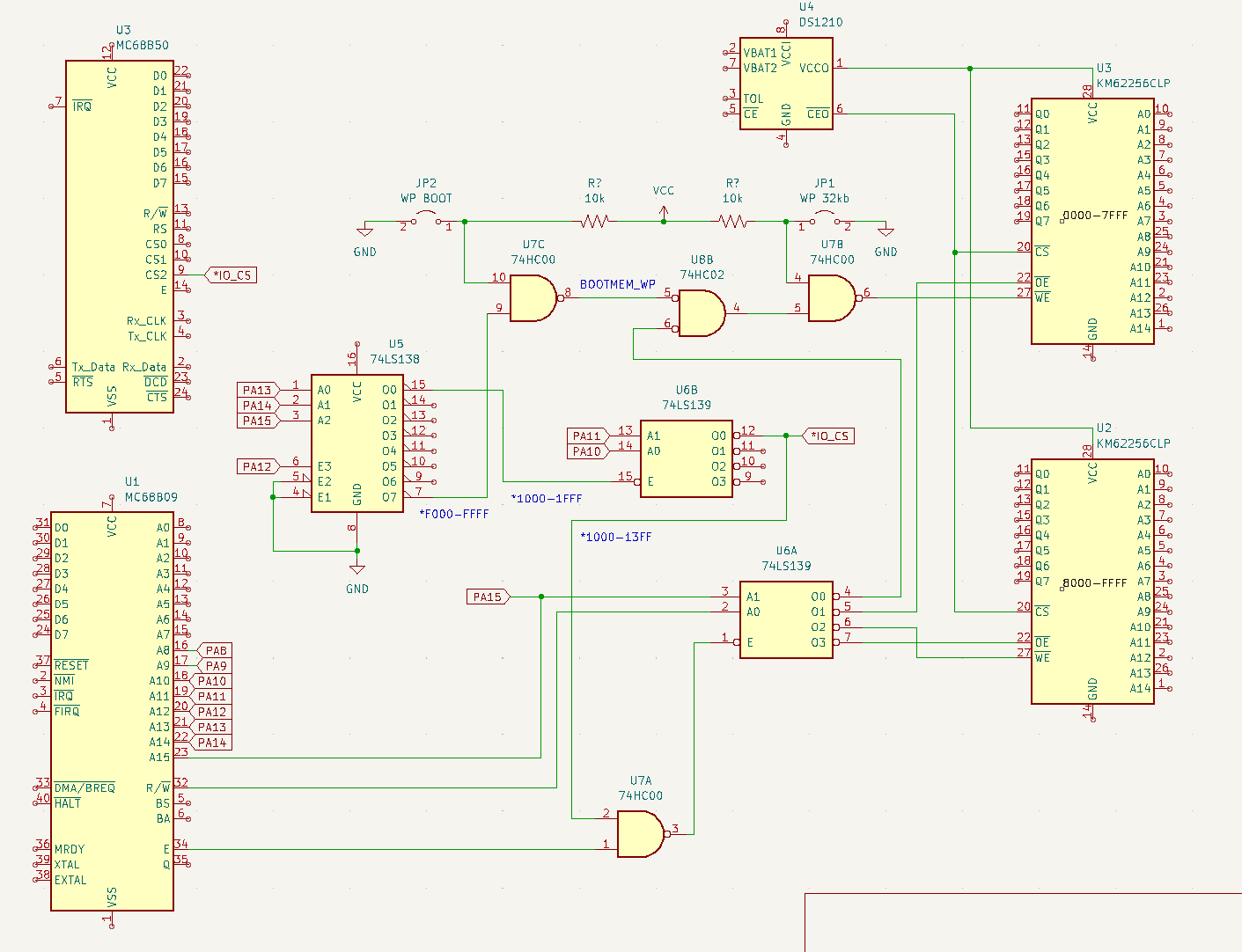
Excellent! Here is a detour I took. Instead of one 512kb RAM with paging, two 32kb RAM. I'm concentrating on address decoding and write protection. It's obviously not finished, but maybe you can see the pattern. Peripherals are mapped in 0x1000 to 0x13FF, the second lowest 1kb of memory space. By placing jumpers on the selector outputs, the I/O could be mapped almost anywhere. All 64kb memory is non-volatile. Either the upper 4kb, or the entire upper 32kb, can be write protected with a jumper. Thus 56kb of contiguous memory is available.
Good idea! A flexible memory map may come in handy.
We just got power back after three days so I've been reading a lot.
Yeah, I've been downloading and reading a lot too. Of course, quickly found the Grant Searle 6 chip design, which was helpful in understanding the SRAM interface. Processor A12 goes to U5 E3 in order to enhance granularity, but it has a side effect that it can only decode odd 4kb pages. I judge that to be an acceptable trade off.
I spent some time thinking about a co-processor back door. It seems, there are many ways but none that leap out as being exceptionally simple. There is
- DMA via HALT, BS and BA
- dead cycle stealing (wait for a processor cycle that doesn't perform a memory access
- interleaved SRAM memory access (these RAM are way, way faster than the processor).
- hardware mailbox registers (no direct access to memory)
Those are the dynamic ones (can communicate with the CPU while it is running). Those can all support simultaneous processor/coprocessor operation. Other interface options exist, but solely for the purpose of loading code.
- Hold reset, grab the bus via buffers/counters from a support MCU
- single step hardware (IIRC you can load memory locations using it)
Finally, a weird idea. Make the upper/lower SRAM selects interchangeable. Then, insert an actual EPROM into the lower slot, boot from it, it loads firmware into the upper SRAM. Then, remove the EEPROM and re-insert the upper SRAM. Or maybe, a "shadow" boot EPROM. IDK.
Remember to have a reset vector at $fffe-$ffff when the processor starts up.
and an IRQ vector at $fff8,$fff9 if any interrupts are expected.
Less obvious, an instruction trap vector at $fff0,$fff1 when using the 6309. It's "reserved" as far as Motorola is concerned... but it will be fetched in cases like illegal instruction or div by zero.
Right. I was just thinking about if you are going to switch an EPROM or some kind of boot rom in and out but yes, you’ll always need a way to react to the vectors.
1 Like
Maybe the 32kb write protect should be software controllable, to emulate a kind of "upload to flash" functionality.
Build a 2-byte ROM out of DIP switches and tristate buffers to hold the reset vector.
... or a diode matrix. I had one card a long time ago.
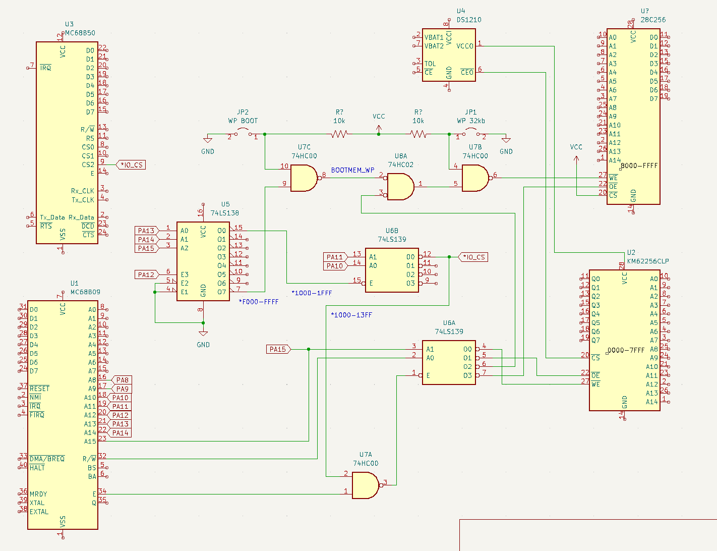
I overlooked the simplicity of writing to EEPROM. So the same circuit can replace one 32kb SRAM with one 32kb EEPROM. It retains the same write protection circuit, so that the 4kb boot section can not be programmed without removing the jumper JP2. The remainder of EEPROM can be programmed in circuit by the processor unless that too is also write protected by JP1.
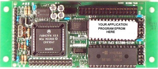
Another significant development. I unearthed a Dallas New Micros HC11 board that I own. It has Forth in ROM, which doubles as a monitor. I thought I lost both the board and the documentation, but luckily no. It's an interesting board in itself, but the key thing is that it can easily read/write JEDEC DIP pinout devices. It looks like this:
So I can do things like
OK
7FC0 40 FF FILL OK
7FC0 40 DUMP
 7FC0  FF FF FF FF FF FF FF FF FF FF FF FF FF FF FF FF
 7FD0  FF FF FF FF FF FF FF FF FF FF FF FF FF FF FF FF
 7FE0  FF FF FF FF FF FF FF FF FF FF FF FF FF FF FF FF
 7FF0  FF FF FF FF FF FF FF FF FF FF FF FF FF FF FF FF
OK
1234 7FFE ! OK
7FC0 40 DUMP
 7FC0  FF FF FF FF FF FF FF FF FF FF FF FF FF FF FF FF
 7FD0  FF FF FF FF FF FF FF FF FF FF FF FF FF FF FF FF
 7FE0  FF FF FF FF FF FF FF FF FF FF FF FF FF FF FF FF
 7FF0  FF FF FF FF FF FF FF FF FF FF FF FF FF FF 12 34
OK
Edit - I count two people here talking about doing this. Anyone else want to try? Features that you would like to see - in keeping with the size and speed of the thing?