I am using an ATtiny 2 series chip for a project. My question is, which of the two sets of RxTx lines are the "standard" UART to which a Serial.println statement will be written when implementing Spence Konde's MegaTinyCore?
The links below were incredibly helpful guides. But In the spirit of "teach a man to fish.." I would be grateful if someone could point out the part I missed that would have answered my question. Konde -Github 1 Konde -Github 2 Arduino Forum
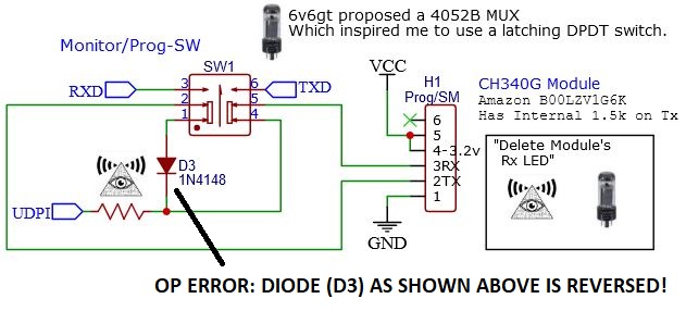
Incidentally I wish to combine monitoring and programming into a single cable. Borrowing ideas from Konde (Dr. Azzy - eye of providence logo) and 6v6gt (vacuum tube logo) see points of attribution in schematic: the image below shows my understanding of how a programming / monitoring switching circuit might be configured. Critical or helpful advice is appreciated!
Update 11/29: As Spence Konde pointed out in his post below, I mistakenly reversed the diode (D3) in the above image. For consistency with Konde's post, I left the original error, and noted it. Konde also mentioned it needs to be a Schottky.
Serial USART0, Serial1 is USART1, RX0/TX0 is for USART0/serial, RX1/TX1 is for USART1/Serial1.
Each of those have the default pinset, and an alternate pinset. This is exposed by Serial.swap() - Serial.swap(1) switches to the alternate pins, Serial.swap(0) switches back to default, and it has to be called before Serial.begin() for us to guarantee that it will work
Also worth noting that the megaTinyCore docs are markedly worse than the DxCore docs now. megaTinyCore has too much stuff in the main file, making it a wall of text that's painful to wade through. As time permits I'm planning to port the docs back - the modern tinies and the Dx-series are very similar.
The pin mapping on the 2-series is... strange in that the alternate pins for Serial and the default pins for Serial1 are the same. I've not yet tried Serial.swap(1) (moving it to the alt pins) and then Serial.begin(115200) and Serial1.begin(115200) - they would then both be trying to use the same pins, and it's not clear whether one of them would "win" or if they'd both be controlling the pins, and in that case what it would mean. And - surely not coincidentally - two of those three pinsets happen to be on the same pins as an the SPI default and alternate mappings - clearly there's some silicon reuse going on under the hood!
The diode in that schematic is backwards - (and it needs to be a schottky diode with the band towards the TX pin of the serial adapter - Serial is idle-HIGH). I tried using one of those mux ICs. My first attempt failed impressively hard and I never got around to figuring out why (my plan btw was to use a 6-pin FTDI header to connect the adapter/programmer board to the target, and have the "CTS" pin on the target actually connected to UPDI. On the latest versions of my breakouts, thats one of the three things that the CTS line can be tied to with solder bridge jumpers. I laid out what I hope will function as an HV UPDI programmer via serialUPDI or a serial adapter. But I'm not getting over-confident, after my previous attempt failed as it did (I managed to totally bung the assembly of >50% of them, one of the worst rates I've had, and the ones that survived that didnt work; I'm not sure if I made a major blunder in the design, or just repeatedly fumbled the assembly.
That said, I've become more or less convinced that you don't actually want the UPDI programmer and the serial monitor to be on the same serial port -you want to be able to have monitor port connected to a serial console, while you upload with another port. Especially on these damned reset-less tinys!
Thanks Spence, for pointing out that error. The ATtiny nets I attached to the push-button must have derailed my focus! (see above, I made clarifications for future forum readers).
Got it. I will do some more experimenting: Using a 1n4148 and no 470ohm resistor, it worked perfectly (to be clear, just the programing worked - I have yet to try the monitoring). However, add in the 470ohm resistor and it fails. Perhaps a 470ohm combined with a Schottky will work. Diodes, I have thousands, but couldn't find a single Schottky! Amazon...
Time Trade-offs: being your own technical writer/curator vs creating cool new technology. One of those is more likely to put a Pyramid-eye shaped dent in the universe. This community seems at the ready to help insulate you from busy work of answering questions that would be solved by optimal documentation.
I am exploring the 14 pin and 8 pin Megatinys. On the 14 pin, two interfaces is fine, nary the twain shall meet.. great idea. But the 8 pin, with an external SPI peripheral, and reading a pot, ugh... I am likely to pivot back to the library-rich world of the old T85, as not enough people have bled to death on the MegaTiny's.
I received your excellent breakout boards yesterday - very well designed!
You've mentioned this before and I'd be curious to see the design for it. I use the one I put together quite intensively and find it useful and it avoids having my desk draped with USB cables etc.
There are, however, a couple of things at least which could be improved:
(1) I should have put a power jumper also in the path of Vcc to the device being programmed to make it easy to force a reset. I'll put such a jumper anyway on any ATtiny1614 boards I make.
(2) I currently have to put a few seconds delay at the beginning of each sketch, if I want to see the initial serial monitor output, to give me time to move the jumper to put the programmer back in the "serial monitor" role.
I have a stack of CH340C chips so I suppose I could put together a programmer incorporating two of them if I ever felt the need to have separate ports for uploading and programming, which you seam to favour.
I was considering a double CH340 board as well. I am in the midst of figuring out fuse issues with a t85, and need an unbricker and programmer on the same board. I thought about using a USB stand-alone hub chip (such as the Microchip TUSB2036, which looks fairly easy to implement) feeding few CH340's, feeding your MUX, all upstream from the Attiny. Another option may be a Quad FTDI (FT4232H) chip, which appears to be a complex bring-up.
Of course this requires a different programmer from the ATtiny 1/2 series.
I did once have the ambition to develop an application onto an ATTiny85 which would have used all 6 GPIO pins, hence no reset pin, and dreamed of a smooth work flow cycle through from developing, testing and resetting with a high voltage programmer. I actually built a programmer to do it. It is here Multiprog v1.0 - Combined HighVoltage + ISP + USBTTL adapter/programmer but, having said that, I do not actually recommend that any one builds such a thing.
(1) The code is horrible due to the design decision I made that I would barely touch any of the existing code I lifted from various sources (A high voltage programmer, the ArduinoISP and some code to drive a Nano as a USB/UART adapter) because I didn't want to test all the mysterious functionality, especially of ArduinoISP, and wanted to leave the code at least recognisable to anyone who needed to modify/debug it. I simply made a framework to wrap each major function. This has the odd effect, for example, that some pins have 3 different names. Also, as far as I remember, I used an obscure library to drive the OLED display.
(2) As I was documenting the work flows for the various use cases, it struck me that, for using all 6 pins of the ATtiny85 there would be so much fiddling with jumpers that the purpose of the whole thing was already defeated. This is when the idea of using an analog switch first occurred to me to simplify this but it was too late for that project.
(3) Last and probably most important is the realisation that squeezing the last GPIO pin out an ATTiny85 is an act of absolute desperation and should only be considered for production runs of many 1000s of a product where the cost savings could justify it. Far better to use the next chip up, in this case the ATtiny84 which I had to do anyway because the ADC on the '85 is was too weak.
I don't believe you need a separate hub to put 2 CH340 chips on the same board. 1 USB cable should do which I think is how passive hubs behave. That is, if you can live with only 500mA at 5 Volts
Back to the UPDI programmer, the analog switch I use, by the way, is the CD74HC4052E not the CD4052B pictured in the schematic. I used the only symbol I could find for the chip and didn't change the name.
I am liking your creation! If I start feeling demoralized by the work flow with HVSP in the loop, it may be a good option to try.
USB device data sheets are sobering reminders of my low station in the world of computer engineering, so I have not examined the CH304 data sheet. Given what you said, I need to have a look. To clear up my understanding, are you saying, for example, that two USB/CH340 modules connected to the PC via a physical Y USB connector would be detected and plumbed by the OS as two COM ports? I would imagine there needs to be a high speed MUX/switch at the Y.
After reading the Microchip data sheet for their TUSB2036 stand-alone hub chip, I was pretty sure it was not a simple physical bus. BTW, it's a pretty cool chip; in practical terms it is a skinless, naked USB hub that you can mount to a PCB. Brewing in my mind is a way to have static com ports that do not vanish when devices are unplugged.