I'm making a project with the Nano Every and I wanted to use a prototype board to solder the components and make it permanent but I didn't find a simple breakout board that would work so I'm making my own and want to ask your opinion which design you like better and if you see any problem or suggestions before I order the PCBs.

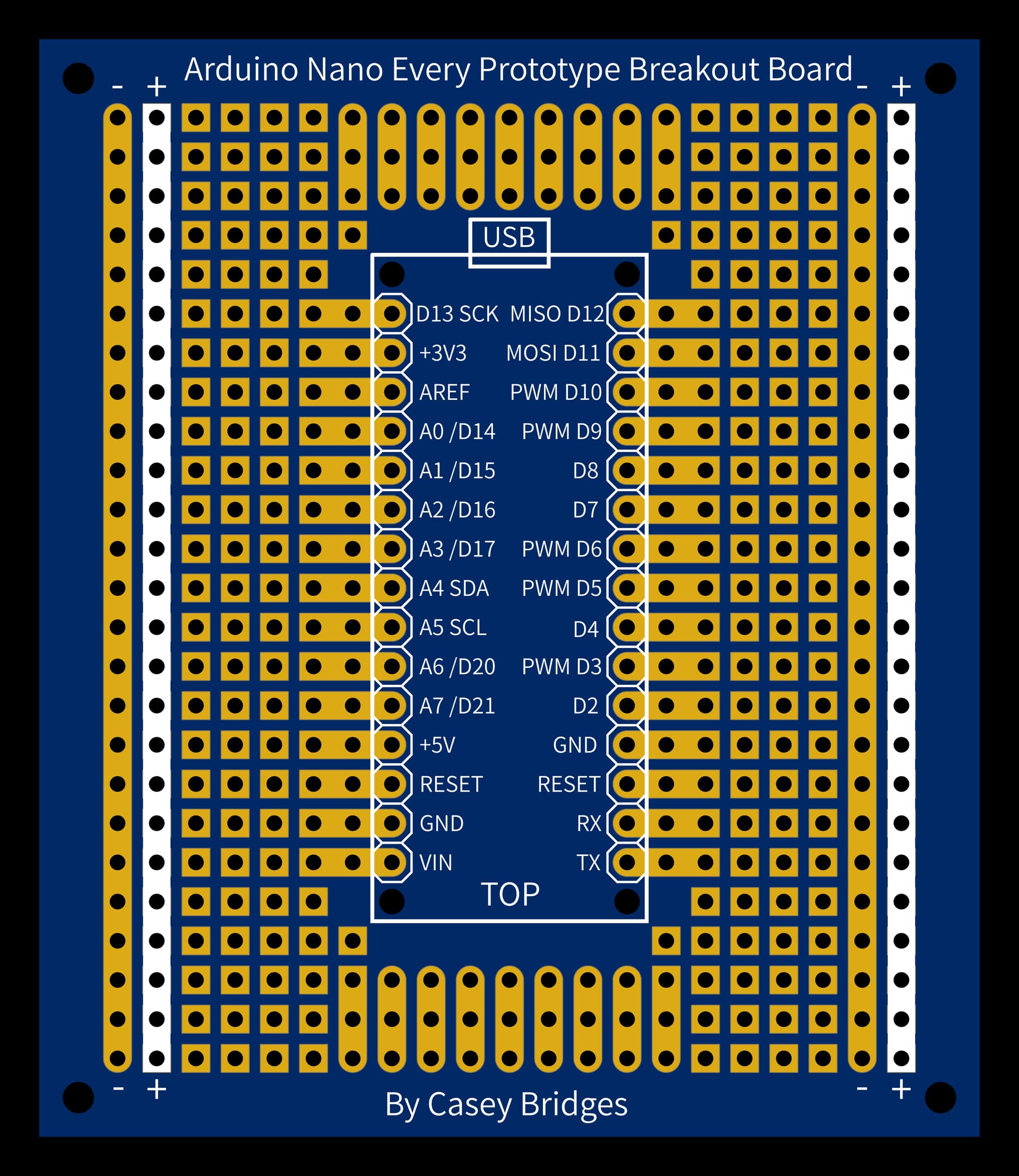
I really dislike the "pad per hole" type prototype boards; you end up with nearly as much wiring to do as plain perfboard ![]()
I don't think it matters what we think, can you fit all the components you want on either board and connect them without a lot of trouble.

This does effectively the same as what you've designed. Why bother making a custom PCB? Just get a pile of the ones in the picture. They cost almost nothing.
I agree with @westfw that you still end up doing lots of handywork with bits of wiring etc. It's an activity that can have a zen-like quality until you power up the board and have to start fixing all the errors.

No meant that the board goes on this side.
Hmm why would you not want a pad per hole? Still new to prototyping
Because then you have to join adjacent pads to connect an Arduino pin to an external connection pin. However, if you use the stripboard style layout of conductors then adjacent holes are already connected and it is easy to break a connection if it is not required
1 Like

I'd also be tempted to move the Nano off into a corner, so that the remaining areas of the protoboard would be big enough for a DIP package, sort-of like:

SMT pads could go on the bottom, underneath the Nano and in the gaps, if desired.
Good Idea
Whats wrong with through-hole
Many Modern parts are not available in TH packages. (although, the same parts are not particularly likely to fit on any pre-made protoboard layout, either.)
It's not about "wrong". Through hole is Legacy, change with industry trends.
@reddragon9, can you let me know what program you used to design the breakout board. I need something similar. Where yould you get them printed/made?
I'm not @reddragon9, but I can strongly recommend you use KiCad to design your PCBs:
There are many different EDA applications, but KiCad is by far the best free open source option available.
The other popular options are proprietary and some will highly recommend them over KiCad. The open source hardware community made the huge mistake of adopting the proprietary EAGLE CAD as the EDA of choice in the early days of the movement's PCB manufacturing phase. The application was well made and provided under a reasonable license so it did what we needed for many years. However, the company that owns EAGLE pivoted to the modern subscription cloud based approach in recent years and so it is now far less suitable of a tool for this community. Since it is a proprietary application, the community had absolutely no recourse other than to either stay locked in, or else have to discard all the application specific knowledge and start fresh with learning the UI of a new EDA application. I hope some lessons were learned from the experience.
1 Like
This topic was automatically closed 180 days after the last reply. New replies are no longer allowed.