Well I worked it out, and I'll document it here in case it helps someone else.
To recap the symptoms:
- I was having trouble uploading to the board using the bootloader
- Once the ASCII table sketch was uploaded only small amounts, or none, of the output appeared in the serial monitor
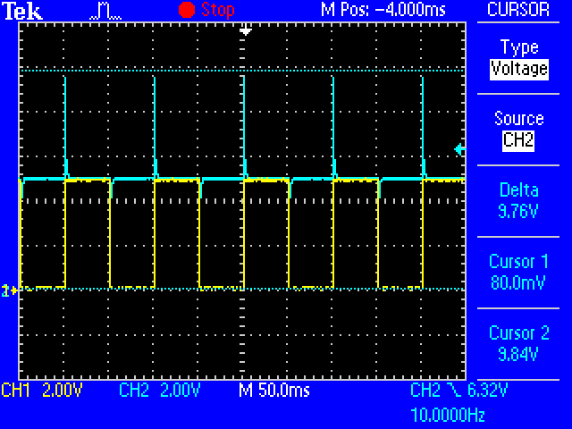
- Further testing showed that the /RESET line dropped to around 1.6V the moment the serial monitor was opened
- Once the serial monitor was closed /RESET went back to 5V
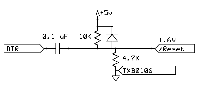
This was the reset circuitry, which should have isolated RESET from DTR. The DTR line is the one brought low by the serial monitor, however the capacitor should have only allowed a pulse through.

A bit of arithmetic showed that the logical explanation for 1.6V on /RESET would be if it was part of a voltage divider, where the "upper" side was 10K and the lower (Gnd) side was 4.7K.
voltage = 4700 / (10000 + 4700) * 5 = 1.6
So basically I needed to find a 4.7K resistor that magically switched itself into circuit when /RESET was pulsed low. And switched itself out when /RESET was pulsed high.
A closer look at the circuit (which I didn't personally design) showed this part, a level shifter which was intended to let the main processor talk via SPI to a transmitter board:
/RESET was going into that chip, however as an input, surely?
Then I read the datasheet for the TXB0106 chip:
Architecture
The TXB0106 architecture (see Figure 1) does not require a direction-control signal to control the direction of data flow from A to B or from B to A. In a dc state, the output drivers of the TXB0106 can maintain a high or low, but are designed to be weak, so that they can be overdriven by an external driver when data on the bus starts flowing the opposite direction.
The output one shots detect rising or falling edges on the A or B ports. During a rising edge, the one shot turns on the PMOS transistors (T1, T3) for a short duration, which speeds up the low-to-high transition. Similarly, during a falling edge, the one shot turns on the NMOS transistors (T2, T4) for a short duration, which speeds up the high-to-low transition. The typical output impedance during output transition is 70 ? at VCCO = 1.2 V to 1.8 V, 50? at VCCO = 1.8V to 3.3V and 40? at VCCO =3.3V to 5V.
Interesting! This chip detects and latches level-changing edges.
The architecture of the chip is shown here:
Note the 4K resistors (circled).
So my theory is now:
-
DTR is brought low temporarily (by connecting the serial monitor)
-
This pulses reset strongly for a moment, through the capacitor
-
The TXB0106PWR buffer chip then decides to "maintain" that signal, weakly, however it is stronger than the 10K pull-up which is there (I calculated that it is, in effect, around a 4.7K resistance, hence the 1.6V)
-
Reset stays at 1.6V indefinitely
-
When the serial monitor is closed DTR goes high which pulses a strong high signal through the capacitor
-
The TXB0106PWR now maintains this new level
In effect, this:
The temporary solution was to cut the trace leading to the TXB0106 pin handling /RESET.
A more permanent one would be, I think, to install another capacitor (circled):

That would let the reset pulse through to the level shifter, but not let the level shifter hold reset low.