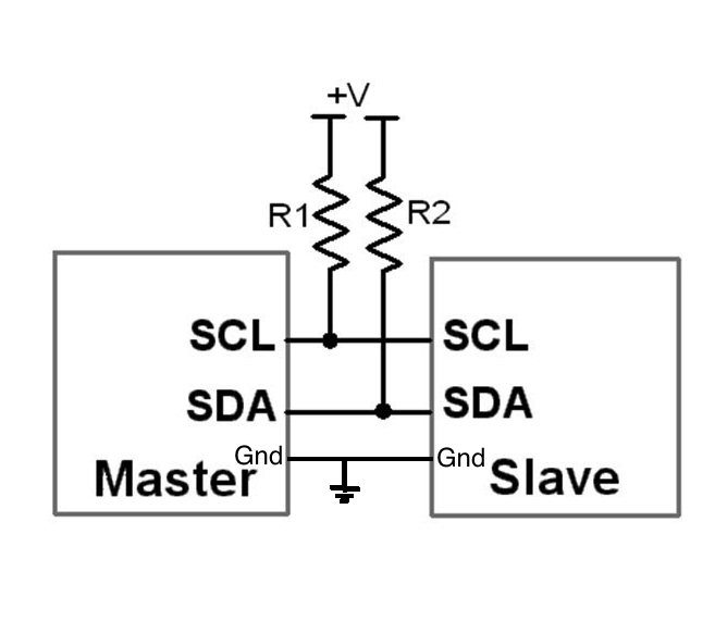
Branching from this thread, I am working on adding 4.7K resistors to my SCL and SDA lines (PCA9685), per @Grumpy_Mike 's recommendation. I've drawn up (chicken scratched) what I think is supposed to be the connection, but it raises some questions.
Are you saying just run the resistors between VCC and the SDA/SCL pins? I assume then, that the signals to the module exist between the resistors and pins?
I2C is an open drain type circuit. The line is held high/to VCC by the resistors.
Signaling is done by the MCU or the device turning on the transistor at its pin, and connecting it to GND. This has the effect of pulling the line down to low.
Note that both (many) devices could simultaneously draw the line down to low without causing harm to any of the others connected to the same line. Obviously, this is an error condition.
Almost true.
It is allowed that one SDAlow is slow and the other SDAlow is fast and that, for example, the SDA overlap while SCL is low. I think that with clock pulse stretching, the SCLlow will also overlap.
A collision detection reads if the data is transmitted properly, that means it checks SDA while SCL is high. The SDA is a "don't care" while SCL is low during the databits (but not during the start- and stop-condition).
The clock pulse stretching is of course a normal valid situation.
The voltage you're pulling up to would be the Vcc voltage used by the parts on each end of the I2C connection. If they are powered at different voltages, I think the lower one would be used.
Yes, pull-ups: tie the SDA and SCL via resistor to +V, the voltage used by the logic.
Info:
SDA and SCL are Open Drain signals. They do not drive an active high, they just pull the lines low. So, the high (when inactive or a bit should be one) comes just from the pull-up.
The value of the resistor depends heavily on the speed you want to achieve. 4.7K might be way too "weak" (too high resistance), even for 100 Kbps.
I use often 2K2 for 100 Kbps, maybe 400 Kbps.
If you want to have 1 Mbps I2C speed - the resistance must be smaller:
The capacitance of the in and output plus these resistors create an RC-circuit. This one is like a low-pass filter, it has a maximum passing frequency. It limits the maximum speed.
You can see the typical capacitor charge periods on scope if R is too large: the signal going high has a ramp and reaches high level "much later", maybe too late for the sampling clock.
Rule of thumb:
The faster the I2C clock - the smaller the resistance - the higher the current the SDA and SCL lines have to draw (when going low).
Assume: I2C signals on MCU can drive up to 20 mA (max.). So, the smallest resistance on a 3V3 logic (CMOS, LVTTL) would be: 165 Ohm.
So, for 1 Mbps speed you might go with 850 Ohms. For 4.2 MHz I use 330 Ohm.
But if you do not need this very high speed, e.g. just 100 Kbps - 2K2 or 1K5 might be OK.
The larger the current (due to lower resistance) - the higher is your entire board consumption (and the MCU pins have a high current load, for draining current into chip, MCU has a total max. for all current on all pins going into chip).
BTW:
Even it is correct to consider the logic level and to put the resistors on the +V rail of the logic with the lowest voltage, there might be a need for level shifters:
If MCU is running with 3V3 and the external logic is also driven by 3V3 - all fine. But if external logic would be 1V8, the pull-ups have to go to this 1V8 (not the 3V3 of MCU) - it can generate issue on MCU input side when reading the SDA line:
The input on MCU is still a 3V3 logic. But the highest level for logic one is 1V8. It might be too low, right at the threshold for a 3V3 input. And the chip would not reliably see a high signal.
In this case - you need a level shifter (bidirectional for SDA line).
Thanks for the additional clarification.
But this too is also almost true. Clock stretching works only if the device supports it, and not every I2C device will do so.
And, in a way, this is also a weakness of the I2C protocol. If the MCU does not have a timeout, this can lead to the MCU hanging up.
In addition, even if the MCU does a reset, the device may still be in a hung state. Troubleshooting can be tricky since it could be any device that is holding the SCL low and there is no easy way to tell which device is causing the problem, esp if it is intermittent.
The simple level shifter is cool. Thank you.
Is there also a simple one for shifting down from 3V3 to 1V8?
"clock stretching": even a feature on I2C, I have never seen a device using it. I do not enable or use.
BTW:
if SCL line is hold low - the meaning is: "I2C bus is occupied" (used by another master).
Actually, the I2C driver in MCU should realize this issue and end via timeout, with error that "bus is busy" (when new transaction tries to grab the bus).
But true seems to be: if a slave device uses clock stretching and holds the SCL line low, right in the middle of an ongoing I2C transaction done by MCU master, but device will not release SCL again - MCU I2C device will hang "forever" (cannot complete). Therefore, I do not like clock stretching.
Additional expert info:
100 KHz, 400 KHz and even 1 MHz are fine. Just to bear the pull-ups in mind.
But I have to deal with I2C devices which support also even faster speed, e.g. 3.4 MHz or even 4.2 MHz.
When it comes to use even faster I2C clock speeds: all above 1 MHz needs a "Master Code":
The Master Code is sent with lower speed, e.g. 100 KHz but it tells the device: the next I2C transaction coming will be with a changed and much faster speed, e.g. 3.4 MHz.
Just as a heads-up (depends your I2C device if faster is possible and MC needed).
Don't make the pull-ups too "weak" (too high resistance): the cable and its lengths acts as a capacitor. And any longer cable needs a smaller resistance value (RC circuit). Best is to check the waveform with an oscilloscope.
In Portenta H7 I have seen: the I2C driver has a short period of time where the SDA, SCL lines are driven as Totem Pole, not Open Drain: they generate for a short period of time a driven high signal of 3V3, coming out from GPIO pin.
This is actually not correct (an I2C pin is always Open Drain, will never drive a high actively). In my case, when connecting a 1V8 logic - it is very risky because for a short period of time the signal level is 3V3.
So, check really with a scope if waveform looks correct, also in terms of fall and raise time of the signals, the low level (e.g. a very strong pull-up might result in: chips cannot tie low enough, the logic low level is too high).
OH YES!
The biggest mistake: you wire all properly but common GND is missing - or weak.
Nothing will work, or is very flaky.
A good common ground (a thick wire, a "star structure", not using analog ground for digital ground) is very important.
GND can be a very tricky issue (a separate topic).