Then you probably have to play around with the source code in GB.ino to make the Cart Reader compatible with this dev cartridge.
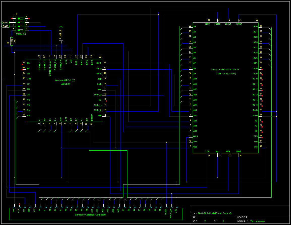
There is a schematic of the cart and also a link to the flash's datasheet here: Tim Hentenaar's Blog
First idea:
If this schematic is correct then the SRAM is connected directly to the cart edge without being controlled by the MBC5-D like you would suspect in a standard MBC5 cartridge.
So that is most likely your problem. The cart reader tries to read data from both the flash and the SRAM at the same time resulting in errors. You need to deactivate the SRAM by not pulling the CE/CS pin low during the read operation by changing the readByte_GB function in GB.ino like so:
byte readByte_GB(word myAddress) {
  PORTF = myAddress & 0xFF;
  PORTK = (myAddress >> 8) & 0xFF;

  __asm__("nop\n\t""nop\n\t""nop\n\t""nop\n\t");

  // Switch RD(PH6) to LOW
  PORTH &= ~(1 << 6);

  __asm__("nop\n\t""nop\n\t""nop\n\t""nop\n\t");

  // Read
  byte tempByte = PINC;

  // Switch and RD(PH6) to HIGH
  PORTH |= (1 << 6);

  __asm__("nop\n\t""nop\n\t""nop\n\t""nop\n\t");

  return tempByte;
}
Second idea: It could be because of the reset pin.
From the datasheet:
3.1 Read
Information can be read from any block, identifier codes, query structure, or status register independent of the VPP voltage. RP# must be at VIH.
The first task is to write the appropriate read mode command (Read Array, Read Identifier Codes, Query or Read Status Register) to the CUI. Upon initial device power-up or after exit from deep power-down mode, the device automatically resets to read array mode.
Five control pins dictate the data flow in and out of the component: BE# (BE0#, BE1L#, BE1H#), OE#, WE#, RP# and WP#. BE0#, BE1L#, BE1H# and OE# must be driven active to obtain data at the outputs. BE0#, BE1L#, BE1H# is the device selection control, and when active enables the selected memory device. OE# is the data output (DQ0-DQ15) control and when active drives the selected memory data onto the I/O bus. WE# and RP# must be at VIH.
Figure 18, 19 illustrates a read cycle.
In the current GB.ino code the reset pin, which in the dev cart is connected to RP#, is not actively driven so you need to change the setup_GB() function so that the reset pin is actively driven high like so:
/******************************************
   Setup
 *****************************************/
void setup_GB() {
  // Set Address Pins to Output
  //A0-A7
  DDRF = 0xFF;
  //A8-A15
  DDRK = 0xFF;

  // Set Control Pins to Output RST(PH0) CS(PH3) WR(PH5) RD(PH6)
  DDRH |= (1 << 0) | (1 << 3) | (1 << 5) | (1 << 6);
  // Output a high signal on all pins, pins are active low therefore everything is disabled now
  PORTH |= (1 << 0) | (1 << 3) | (1 << 5) | (1 << 6);

  // Set Data Pins (D0-D7) to Input
  DDRC = 0x00;
  // Disable Internal Pullups
  //PORTC = 0x00;

  delay(400);

  // Print start page
  getCartInfo_GB();
  showCartInfo_GB();
}
Third idea: The flash chip has two banks controlled by the MBC5-D, if you're lucky the MBC5-D switches the flash's banks automatically, but it could also require a special command to switch the banks. You probably would need to hook-up a logic analyzer to find out if that is the case.