... a month has passed. And still no PCB available, but, one step after the other ... ![]()
First of all - what a surprise ![]() - I'm not the only one who has faced the task to get a voltage controlled current source, which is also refered to as a electronic load, running.
- I'm not the only one who has faced the task to get a voltage controlled current source, which is also refered to as a electronic load, running.
Unfortunately a lot of schematics are shown to make it work, but rationales for the design are rare ... A very good inspiration has been shared here in EEVblogForum. One eye-opener has been that almost every schematic shows an integral controller while not naming it as such, but in the EEVblog-Forum it became visible... and I was beamed back into known territory ![]()
But again, it was not clear how(!) the parameters of the critical components have been found. So I started reading in a book from university on how to model arbitrary electronic networks with just passive components and controlled sources (as it would be needed to model the MOSFET). And had to extend the given theory on my own. The professor wrote "... extension is straight forward as outlined in previous chapters" - uh, not that straight forward I can tell.
Why? Because than I can play with the parameters and see the effect of it ...
So I was setting up several models, of a MOSFET, of a wire as transmission line, an 2nd-order OpAmp to properly catch OpAmps phase shift at unity gain, have renewed my MATLAB license and bought the control toolbox ... and did my investigations in frequency domain (luckily the system turned out to be minimal-phase, root locus analysis as the-otherwise-to-use method would be not that comfortable for given problem).
Please consider the schematic below:
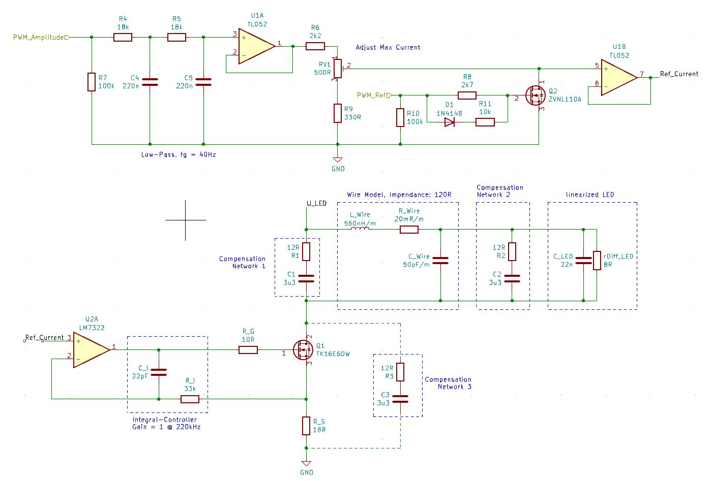
What to see:
-
In the upper part the generation of reference current. The already discussed 2kHz PWM enters at PWM_Ref, its desired amplitude at PWM_Amplitude. R8, D1, R11 are to form symmetrical rise and fall times (not finally choosen yet)
-
In the lower part the components of the current controller including wire and LED. Boxes show the elements. Compensation network 3 is actually not part of the model, but network 1. I consider location of network 1 as more feasible as AC-wise both networks are at same location, but network will allow a PCB design for which the current running through network one will not enter the PCB as far as it is excited the wiring when placed at close to the wire-terminals.
What are the design rules, well what I found is:
-
R1 starts acting reliable when less than 20% of wire impedance. In the circuit it is 10%.
-
Time constant R1.C1 shall in the range of one formed by R_Wire and L_Wire. In the schematic there are equal.
-
Compensation network 2 is not adding really something when it comes to stability of the circuit
-
Without compensation network 1, stability of circuit can not be achieved for all (considered) variable parameters
-
Phase margin is excellent (close to 90°) provided the gain of the I-controller drops below one at least one decade below gain bandwidth of OpAmp
-
High MOSFET capacitances lower phase margin, but still good. Despite - I have a question on this, see below.
-
Effect of wiring inductance is, when designed as above, almost elimated (ok, im my calculations). I have a question on this, please see below.
-
Highest "risk" of unstable control loop is when LED shall be off (--> high differential resistance of LED).
To share some result, see picture below with, but some remarks up-front
-
uShunt is voltage accros R_S
-
Phase and Gain are given for closed loop transfer function
-
Just as indicator (can be actually better seen in open loop transfer function), "trouble" starts at around 1MHz
-
For sure, at the upper range of shown frequency range my model is to simple by far
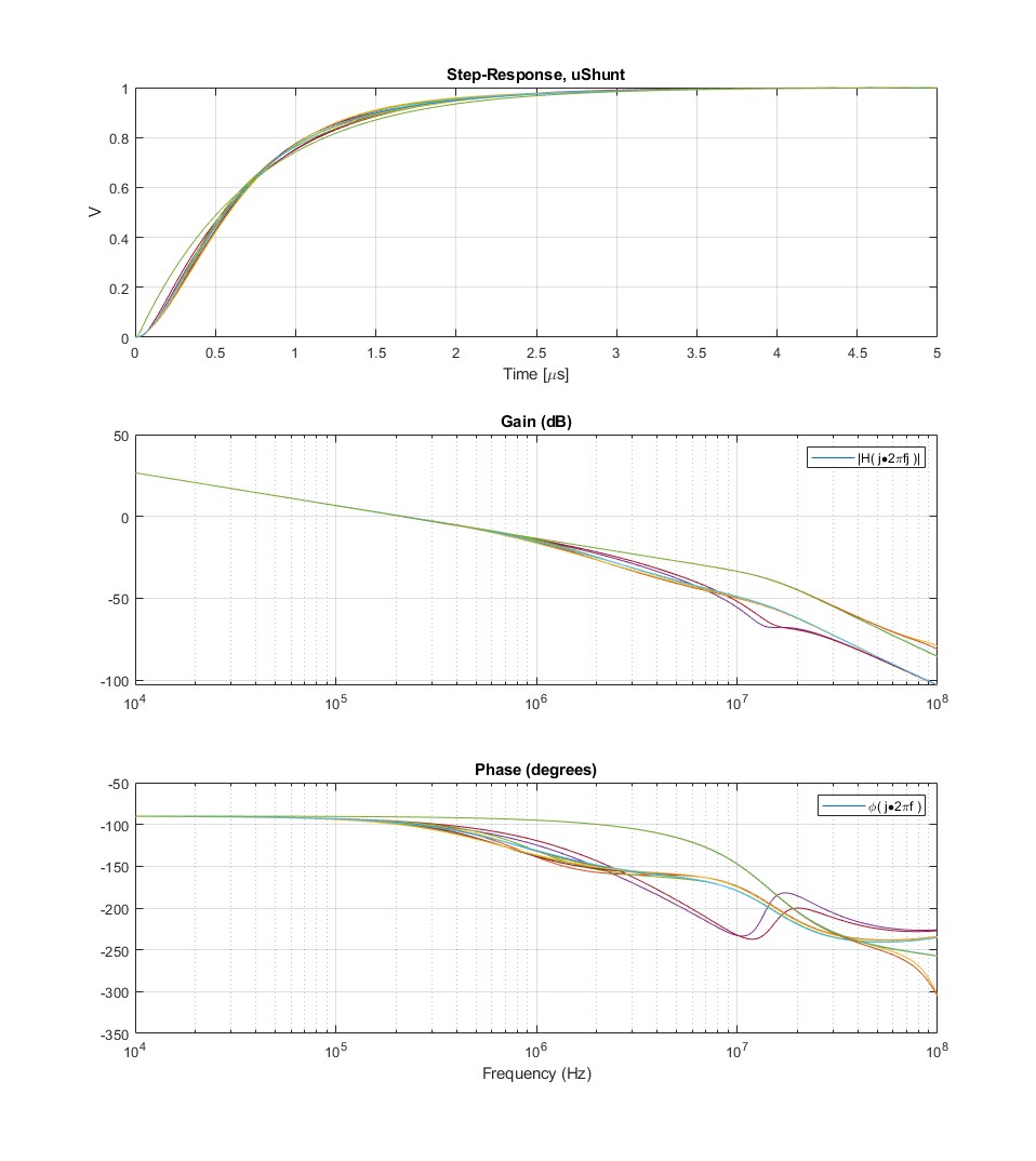
The following parameters have been varied:
-
Length of wire (0.1 to 12.1 meters)
-
Differential resistance of LED (10^-1 ... 10^4 times resistance when LED is on)
-
MOSFET capacitances at 0.1V, 3V, 40V at data sheet value (covering LED on, off, and extremes)
-
Forward transonductance of MOSFET is hard to get out of data sheets (at least for the considered one). So a sweep with 1, 10 and 100S
NOW, my questions:
-
I'm not that sure about values taken for the wiring (see schematic). Are there other I should take into account? Load current is below 150mA, you see my wire gauge selection indirectly by selected resistance of 20mOhm/meter.
-
What, for later test, will be better: twisted, or un-twisted?
-
I struggle a little with the compensation network. As you can see, e.g., R1 is low. With U_LED = 40V the current through the MOSFET is 40V/12R = 3.3A worst case, even though just short. Looking into the SOA of the MOSFET TK16E60W or in alternative MOSFET TK6A60W, which I would prefer due to lower capacitances ... but I'm not sure.
Basiscally, last question is that I'm not sure on how to read data sheet properly when it is not about single pulse.
Your support is appreciated.
Ah, I forgot to add: Push-Pull is not forgotten.