Hi
as announced in #8 it took some time to take care about your tipps on how to further investigate the observed phenomenon.
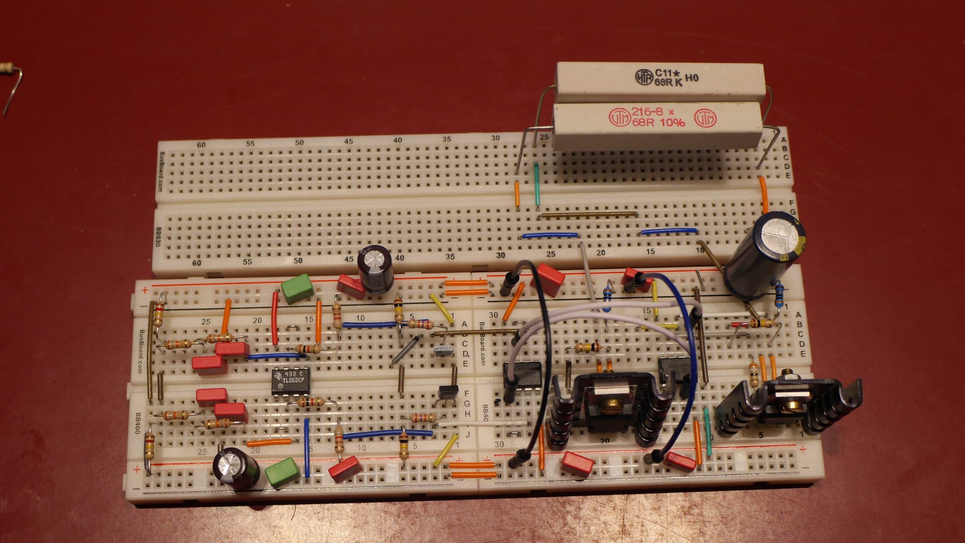
Improving the routing of ground (GND) on breadboard was significantly changing the measurements. See below a picture of the breadboard with in 5 connections between the upper-GND-busbar and the lower-GND-busbar (which is indicated by + in red, don't get confused). Most effect has the one close to the OpAmp driving the MOSFETs on the very right on the picture (green and brown wire).
Usage of scope ground connection as recommended by @anon57585045 . Which I have taken actually also as advise to improve the grounding on the breadboard as well.
With respect to use 10x probes I think I did something wrong (not sure). I haven't told the scope that the probes are configured in 10x, i.e. I had increased the input sensitivity instead. So far I just have seen that, while measuring on more than one channel, all probes should be configured the same (either all 1x or all 10x, but not mixed). Nevertheless, in the way I did it I did not observe a difference between the measurements (i.e. with same conditions 1x and 10x)
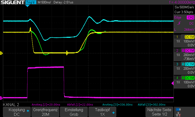
PURPLE: Signal to turn current OFF (output function generator)
YELLOW: Input to voltage controlled current source (CW_Ref) in circuit shown in #1. As such, it goes down to zero when the signal to turn current off gets HIGH. I.e. acts as reference value
GREEN: Measured current across shunt resistor R42. Shall match with yellow one. I.e. acts as acutal value. GREEN shall follow YELLOW.
BLUE: output of driving OpAmp U16A.
So, what to see:
oscillation is mostly gone!
For remaining oscillation I noticed that, with reference to blue curve during switching current on again that there is a linear rise of OpAmp's output voltage. Rise is about - no kidding - 7V/s, which is OpAmp's maximum rise time as per data sheet. I.e. I think oscillation is actually not caused by low phase margin rather non-linear behaviour of OpAmp.
Ok, still to fast but on the limit of the OpAmp. Measured current (green) catches up with the yellow during turn on, then some "recovery" in the closed loop as Gate voltage for MOSFET was to high (but delayed due to limited rise time!), so output current had to catch up again ...
So, I think, I either accept the oscillation (as know it is better understood), or try to find an OpAmp with higher dv/dt, and probably slow down the switching in general.
Note: Pulse width at 2kHz PWM has been adjusted to look nice on one screen both rising and falling, but was a little longer than final pulse width to be used.
Let me try to answer.
First off all I try within my light project, which included dimming of the LED, to take latest research into account that is dealing with the dimming of LED and is related physical effect on humans.
IEEE has publised an investigation back in 2015 on Recommended Practices for Modulating Current in High-Brightness LEDs for Mitigating Health Risks to Viewer (IEEE 1789).
In short, high modulation at low frequencies are bad (except for rock - concerts ). IEEE 1789 Paper (have a look on page 44)
Modulation of a PWM is always 100% (full on, full off), i.e. highest possible, i.e. most worse. While modulation of a DC signal is 0%, it does not changes its value at all, thus lowest possible and therefore best choice.
Additionally frequency play a role. The higher the modulation the higher the frequency has to be in order to have health risks mitigated. For PWM, frequency has to be at least 1.1kHz (that's why I use 2kHz, which is closed above 1.1kHz an ATmega328 can provide (or at least I was able to find the proper register settings for)).
Now, why using PWM in lower current range. In general, High-Power LEDs are made of several small LEDs. And those small LEDs are not all totally identically, which becomes visible when operated below their rated current.
So to cope with this, the driving scheme switches from current driven to PWM driven at lower current range.
You may say: this is all overdone. Well, probably, but as written in the beginning, I'm a little ambitious to build the best possible also with respect to human's preception of the light. And, to some degree, it is also a little competition to what is commercially available. I know only one manufacturer who fullfills IEEE 1798, the majority uses PWM frequencies below 1.1kHz.
Some remark: IEEE 1798 might not be totally true in that sense that their approach is really covering interaction between a dimmed LED and a human. There exist others, however they haven't been put into a final recommendation of what to do (or I didn't find). Additionally, EU is not following IEEE 1798 but simultaneously does not provide an alternative for dimmed LEDs (so far just for LEDs fully on).
Hope that answers all your questions.
Ah, hold on:
Yes, I want to created a human centric light (HCL) for my home office. That is, colortemperature follows the sun during day, warm white in the morning, cold white at noon, warm white at the evening again.
I have no means to meaure it. 0.5W metall film resistor. You can find the resistor on the top right of the breadboard. The resistor right next to the big capacitor.
As with respect to the 10x probes: I will check with proberly configured the scope as well. I had to remove my test setup to reply here in the forum (don't have an extra bench for that).
There is a 10x/1x switch on the probes, in addition to the setting on the scope. To use it properly, you have to perform the calibration adjustment of the adjustable capacitor on the probe. The procedure would undoubtedly be documented in the scope manual.
But, aren't you overthinking this whole thing? You're passing a high speed digital signal through a slow op amp circuit, and the output is slow. That is normal. There is no harm in running one channel on 1x and the other on 10x, if each channel is configured correctly.
If your probe is correctly connected to a low impedance source like a low value resistor, in fact it makes no difference whether you are using 1x or 10x settings. In that case, the additional cable capacitance of the 1x arrangement does not affect the signal very much at all. When I told you earlier on, to use 10x I was just trying to rule out unknown errors (as there are some facts that weren't posted then).
The ringing you see is not likely caused by non-linearity in the op amp. It's caused by the reactance of the load and feedback circuit.
Sure, it is. Things get slow when the out of an GPIO hits anlogue circuits. I'm fine with this.
Well, I interpretation is exactly this. Have a look on the blue curve. This is not the response of a linear system with the "yellow signal" at its inputs. To be seen at the different slops left and right to the maximum on the blue curve in the middle of the shown measurement. Well, to be confirmed - I'll investigate and wait for other OpAmps (ordered but not delivered yet).
Ah, not those monster-resistors I just had in my big box of unsorted elements. In their current-capabilities totally oversized - I drive the test at about 100mA, which is close to final.
Sorry, wrong description. The shunt is right to the big capacitor in the middle right of the picture. The two big ones I use to simulate the load. And, as said, are totally oversized... but work so far ... in case they cause the oscillations I'll track this. As decribed somewhere above, I'm slowly increase complexity of my test set-up to always know what is new and then to properly understand new effects (if there are some). Better then putting all together from the very beginning having various parameters that can drive things not working ...
Like everybody does - I think. Have to a tunable white LED with actually two LEDs build-in differing in their color-temperature (e.g. 2800K and 6500K). Linear interpolation inbetween, which creates color error, but this is another story ...
I see that, but why go to linear control at near full luminosity, that is where your efficiency will be the lowest, keep PWM all the way to 100%.
Have you tried just controlling from 0% to 100% PWM?
Also check you scope menu, if you are using x10 probes, then you should be able to tell the scope that it is connected to x10 and it will adjust the range scale appropriately.
It should, I use 30yo scope at work and it does.
As I was trying to say I prefer DC / no PWM with respect to interference with human's perception. So efficiency is not at first priority. So, yes, efficiency is not as good - but with given components (DC power supply of (42V), LED voltage drop (around 36V at full current), the effiency is about 36/42 = 86% still good. Only 6V used for the MOSFET and Shunt resistor are waste ... 6V out of 42V.
No, for reason just stated above. Additionally I can not avoid to have wiring between my LEDs and my electronics driving the LED. So, from EMI point of view I also try to avoid EMI as far as possible - or to left this to low currents, at least.
Frist (@DrDiettrich, @anon57585045 , @TomGeorge), I have now properly calibrated my probes to 10x and also configured my scope accordingly. Sorry to run this twice as I haven't used to 10x-option in the past. Now it works fine!
Why going back? I revealed some non-linear behaviour of the voltage current source, which first let me believe it is all fine, but, well, no ...
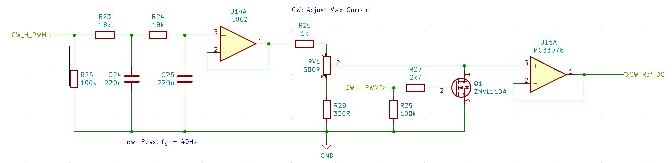
To allow you to follow please have a look on schematic below first:
DAC from PWM-output by means of simple low-pass. Output of U14A is proportional to load current at 100%.
Lowering reference voltage to be measured across shunt resistor. Shall be 2V at 100% load current.
Q1 is used to apply PWM when desired (running at 2kHz)
Output if buffered by U15A, and will is fed into voltage controlled current source shown in #1
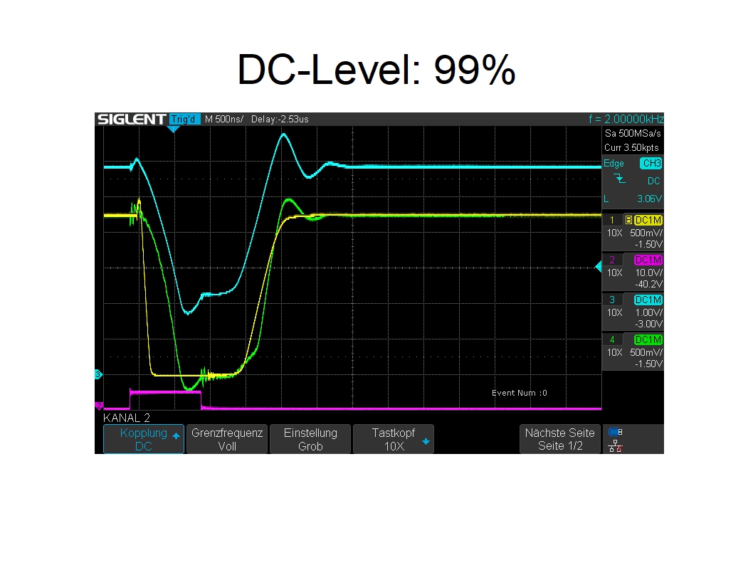
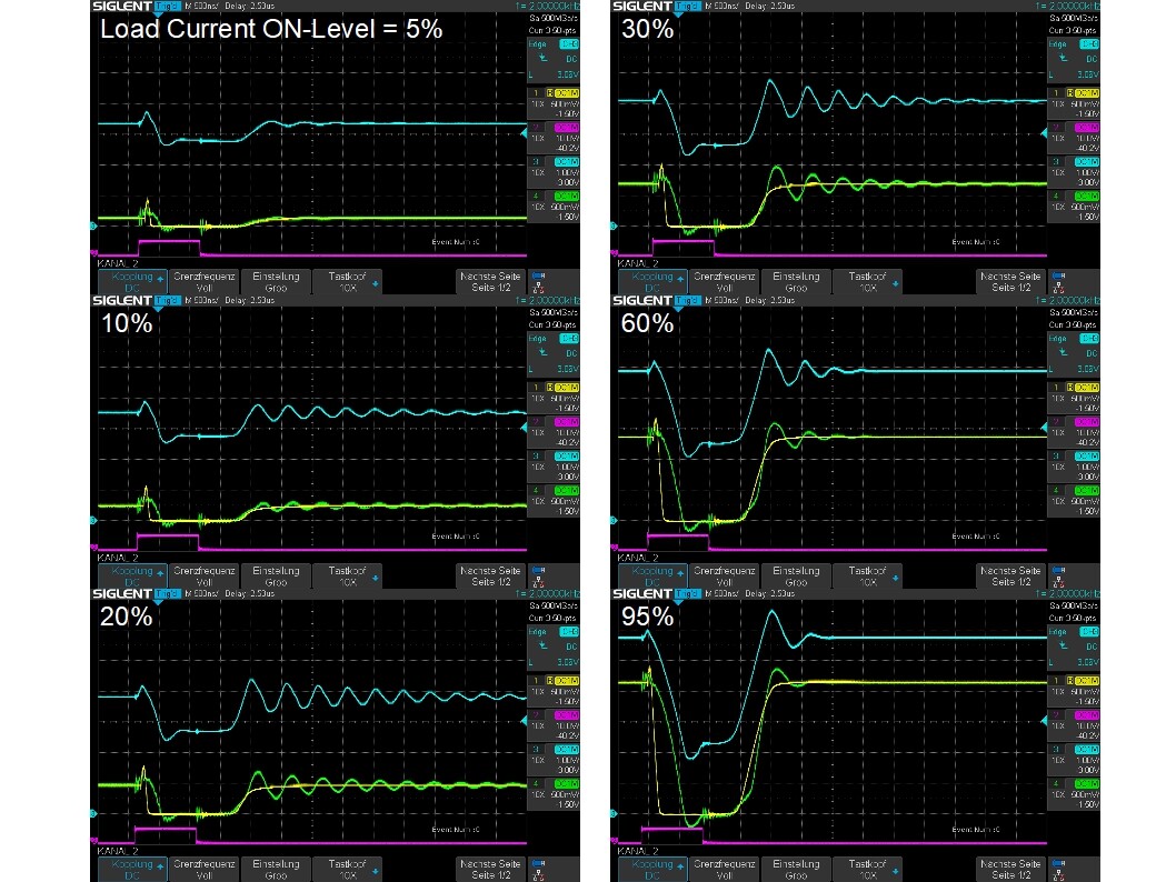
Have a look at one measurement (10x probes, all probes with individual GND-connection as close as possible, Coax-Cable from function generator, thick wiring from labatory supply).
Colors as before. GREEN shall follow YELLOW. BLUE is driving voltage for MOSFET. PURPLE command to switch MOSFET off (CW_L_PWM)
Well, then I changed the duty cycle of the just shown schematic to set different load currents (i.e. of the signal CW_H_PWM. The higher the duty-cycle, the higher the amplitude of CW_Ref_DC.
Then I got this (all settings on the scope unchanged):
That's kind a strange, isn't it? At both lower (5%) end upper end (95%) of load current oscillations a well damped. Then, with increasing duty cycle damping gets less to increase again for duty cycles above 30%.
I swear, I haven't touched and wiring during the measurements.
Please note I was able to get scorpe's grid on the screen. So with 500ns/div oscillation is about 2MHz.
Any idea why dynamic behaviour may depend on current levels?
I think the ap amp is driving heavy capacitive load. R39 makes this worse because it forces the op amp output to overshoot to quickly reach the target. As mentioned previously the op amp output saturates, which badly degrades its performance and so it overshoots a lot before it gets back into regulation. Trying to correct the overshoot it saturates in the other direction.
I don't know why this oscillate less at current extremes. It is interesting observation but I don't think a single cause can be found - it may be combination of many subtle factors. As long as the oscillation is damped I don't think it does matter. You may try to show down the change of the reference and increase speed of the op amp by removing R39.
Matter of fact, I don't think so. Why?
Q3 is configured as source-follower, that is the gate capacitance is bootstrapped (both plates of Cgs move (almost) by the same amount of input voltage because gain of source follower is (almost) one. So input capacitance becomes just
Cin = Cgd + Cgs / (1 + gm*Rs) with Rs = R42. Having gm for sure above 1S (or some low 2 digit number) Cin is approximately Cgs
Honestly, I had toughts in the same direction. But then I figured out that Q3 is running as source follower and concluded that capacitiy load to OpAmp shouldn't be a problem because it is loaded with just (small) Cgd.
Does your proposal still holds taking the source follower into account? Despite, I would need a sketch because I don't understand exactly would you mean ... sorry.
One thing - it's not exclusively a source follower if the voltage on the drain is of opposite AC polarity to the voltage on the gate. That will induce some negative feedback through the parasitic drain to gate capacitance.
With any such circuit that relies on closed loop control, the op amp feedback loop includes all the reactance of the driven circuit that is included in it. So compensating it can be tricky if the reactance is high. The higher the loop gain, the more stability becomes a problem and a voltage follower is a worst case for that.
I'll see about a drawing, but actually there are different implementations of buffer amplifiers that you could use there, any would work so it's a generic design problem and my solution wouldn't be particularly special.
Regarding your scope shots, it's not clear to me exactly where in the circuit you have connected the probes (especially the blue and green, which I assume are somewhere in the output stage).
This I can quickly answer:
BLUE: Output pin 1 of U16A. So it can be seen that output of OpAmp does't saturate but slew rate can be observed.
GREEN: at source of Q3, i.e. voltage across shunt resistor R42. That's why I write GREEN follows YELLOW, which is CW_Ref / Pin 3 of U16A
I agree. And for that reason I was thinking to replace load resistor (the big 68R resistor) by a Zener-Diode (as simulation of LED) because voltage drop across LED is "more constant" for variable load current then for the resistor I'm using. Load resistor would be replaced by differential resistor of Zener/LED, being much lower than the 68R I'm using now (e.g. voltage drop is changing across zener by 1V for 0 to 0.1A it would be just 10R, so reducing the effect of negative feedback you are refering to, right?