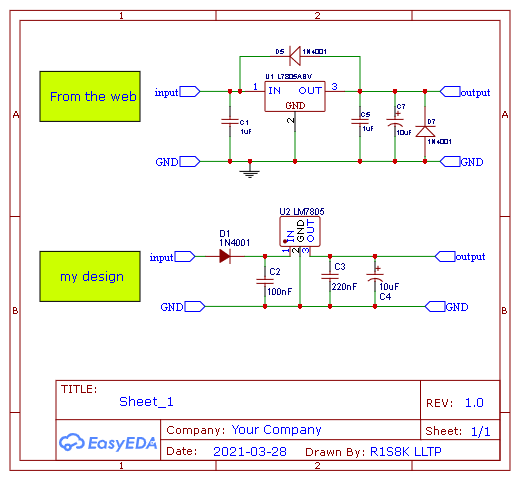
I ran by this design from a website and I noticed the use of two diodes in the design and I know they are for protection.
But can anyone explain to me why each one is placed in that position.
Also I put my design with it and I want to tell if my design is enough or the other one is better.
D7 protects the circuit when there is no load to discharge the decoupling capacitor.
I believe D5 is part of that protection as well but I am not certain as it might also serve as short protection for the input voltage.
I guess it depends on what you're trying to protect against. In the "web" design D2 would protect against reverse voltage at the regulator output (which would have to come from "somewhere else". D1 protects against "back powering" the regulator. That could be from somewhere else, or it could be a "large" filter capacitor on the output.
Your design protects from a reversed connection on the input. You also get a small voltage drop across the diode, which could be a good thing if you have lots of voltage on the regulator input and you are stressing the regulator. It could be a bad thing if you have barely enough voltage on the input.
Yes. In the first diagram ("From the web"), D5 protects the regulator chip from the situation where the OUT terminal become positive with respect to the IN terminal. This happens when the input voltage disappears (i.e. pin 1 goes to GND), but the charge in capacitors C5 and C7 maintains a positive voltage on the OUT terminal. This can damage a 78-series regulator. D5 allows C5 and C7 to discharge via the (now at 0V) input wire.
D7 protects the circuit connected the output from reverse polarity. If the input polarity is the wrong way round, so GND is positive with respect to input, then D7 and D5 put a near-short circuit across the supply, blowing the fuse further back up the line, protecting the circuit connected to the output.
In "my design', D1 protects the regulator and the circuit connected to the output from reverse polarity of the input. However, this comes at the cost of dropping 0.6V or more across the diode in normal operation. In this circuit, switching off the input cannot pull the IN terminal of the regulator down to GND potential because D1 prevents that, and the charge on C2 holds the IN terminal positive until the circuit connected to the output has discharged C3 and C4.
So "my design" does the same job as "From the web", but with one less diode, at the cost of 0.6V-odd dropped across D1 in normal use.