Hi @bastenhoor,
Okay, here is the Arduino IDE version.
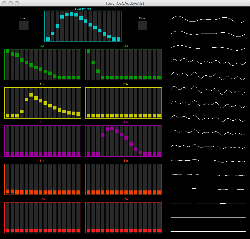
Tone fundament is selected by a voltage (i.e. pot) on A1 between 27.5Hz (piano note A0) and 4123.5Hz (note C8).
/* Arduino UNO R4 example code - Sound Synthesis
* Using Timer 7 interrupt at c. 44.1kHz
* Super-Fast sine calculation of frequency and harmonics from ADC value
* With fast non-blocking ADC analog-read and DAC analog-write operations
*
* Susan Parker - 6th April 2025.
*
* Realtime sine calc with Paul Stoffregen's 11th order Taylor Series Approximation
* https://www.pjrc.com/high-precision-sine-wave-synthesis-using-taylor-series/
* Note: I have condensed the Taylor Series code to a single set of inline asm calls
*
* This code is "AS IS" without warranty or liability.
* There may be glitches, etc. please let me know if you find any; thanks.
This program is free software: you can redistribute it and/or modify
it under the terms of the GNU General Public License as published by
the Free Software Foundation, either version 3 of the License, or
(at your option) any later version.
This program is distributed in the hope that it will be useful,
but WITHOUT ANY WARRANTY; without even the implied warranty of
MERCHANTABILITY or FITNESS FOR A PARTICULAR PURPOSE. See the
GNU General Public License for more details.
*/
// ARM-developer - Accessing memory-mapped peripherals
// https://developer.arm.com/documentation/102618/0100
/* Start of Register Definitions - Use Code Folding to collapse these with V to > select (next to line numbers) */
// ==== Interrupt Control Unit ====
/* Default Arduino Startup - see section 13.3.2 for Event Number info
0 33 USBFS_USBI
1 34 USBFS_USBR
2 31 USBFS_D0FIFO
3 32 USBFS_D1FIFO
4 1E AGT0_AGTI
...
*/
#define ICUBASE 0x40000000 // ICU Base - See 13.2.6 page 233
// 32 bits -
#define IELSR 0x6300 // ICU Event Link Setting Register n
#define ICU_IELSR00 ((volatile unsigned int *)(ICUBASE + IELSR)) //
#define ICU_IELSR01 ((volatile unsigned int *)(ICUBASE + IELSR + ( 1 * 4))) //
#define ICU_IELSR02 ((volatile unsigned int *)(ICUBASE + IELSR + ( 2 * 4))) //
#define ICU_IELSR03 ((volatile unsigned int *)(ICUBASE + IELSR + ( 3 * 4))) //
#define ICU_IELSR04 ((volatile unsigned int *)(ICUBASE + IELSR + ( 4 * 4))) //
#define ICU_IELSR05 ((volatile unsigned int *)(ICUBASE + IELSR + ( 5 * 4))) //
#define ICU_IELSR06 ((volatile unsigned int *)(ICUBASE + IELSR + ( 6 * 4))) //
#define ICU_IELSR07 ((volatile unsigned int *)(ICUBASE + IELSR + ( 7 * 4))) //
#define ICU_IELSR08 ((volatile unsigned int *)(ICUBASE + IELSR + ( 8 * 4))) //
#define ICU_IELSR09 ((volatile unsigned int *)(ICUBASE + IELSR + ( 9 * 4))) //
#define ICU_IELSR10 ((volatile unsigned int *)(ICUBASE + IELSR + (10 * 4))) //
#define ICU_IELSR11 ((volatile unsigned int *)(ICUBASE + IELSR + (11 * 4))) //
#define ICU_IELSR12 ((volatile unsigned int *)(ICUBASE + IELSR + (12 * 4))) //
#define ICU_IELSR13 ((volatile unsigned int *)(ICUBASE + IELSR + (13 * 4))) //
#define ICU_IELSR14 ((volatile unsigned int *)(ICUBASE + IELSR + (14 * 4))) //
#define ICU_IELSR15 ((volatile unsigned int *)(ICUBASE + IELSR + (15 * 4))) //
#define ICU_IELSR16 ((volatile unsigned int *)(ICUBASE + IELSR + (16 * 4))) //
#define ICU_IELSR17 ((volatile unsigned int *)(ICUBASE + IELSR + (17 * 4))) //
#define ICU_IELSR18 ((volatile unsigned int *)(ICUBASE + IELSR + (18 * 4))) //
#define ICU_IELSR19 ((volatile unsigned int *)(ICUBASE + IELSR + (19 * 4))) //
#define ICU_IELSR20 ((volatile unsigned int *)(ICUBASE + IELSR + (20 * 4))) //
#define ICU_IELSR21 ((volatile unsigned int *)(ICUBASE + IELSR + (21 * 4))) //
#define ICU_IELSR22 ((volatile unsigned int *)(ICUBASE + IELSR + (22 * 4))) //
#define ICU_IELSR23 ((volatile unsigned int *)(ICUBASE + IELSR + (23 * 4))) //
#define ICU_IELSR24 ((volatile unsigned int *)(ICUBASE + IELSR + (24 * 4))) //
#define ICU_IELSR25 ((volatile unsigned int *)(ICUBASE + IELSR + (25 * 4))) //
#define ICU_IELSR26 ((volatile unsigned int *)(ICUBASE + IELSR + (26 * 4))) //
#define ICU_IELSR27 ((volatile unsigned int *)(ICUBASE + IELSR + (27 * 4))) //
#define ICU_IELSR28 ((volatile unsigned int *)(ICUBASE + IELSR + (28 * 4))) //
#define ICU_IELSR29 ((volatile unsigned int *)(ICUBASE + IELSR + (29 * 4))) //
#define ICU_IELSR30 ((volatile unsigned int *)(ICUBASE + IELSR + (30 * 4))) //
#define ICU_IELSR31 ((volatile unsigned int *)(ICUBASE + IELSR + (31 * 4))) //
// IRQ Event Numbers
#define IRQ_NO_EVENT 0x00
#define IRQ_PORT_IRQ0 0x01
#define IRQ_PORT_IRQ1 0x02
#define IRQ_PORT_IRQ2 0x03
#define IRQ_PORT_IRQ3 0x04
#define IRQ_PORT_IRQ4 0x05
#define IRQ_PORT_IRQ5 0x06
#define IRQ_PORT_IRQ6 0x07
#define IRQ_PORT_IRQ7 0x08
#define IRQ_PORT_IRQ8 0x09
#define IRQ_PORT_IRQ9 0x0A
#define IRQ_PORT_IRQ10 0x0B
#define IRQ_PORT_IRQ11 0x0C
#define IRQ_PORT_IRQ12 0x0D
// IRQ_PORT_UNUSED 0x0E
#define IRQ_PORT_IRQ14 0x0F
#define IRQ_PORT_IRQ15 0x10
#define IRQ_DMAC0_INT 0x11
#define IRQ_DMAC1_INT 0x12
#define IRQ_DMAC2_INT 0x13
#define IRQ_DMAC3_INT 0x14
#define IRQ_DTC_COMPLETE 0x15
// IRQ_UNUSED 0x16
#define IRQ_ICU_SNZCANCEL 0x17
#define IRQ_FCU_FRDYI 0x18
#define IRQ_LVD_LVD1 0x19
#define IRQ_LVD_LVD2 0x1A
#define IRQ_VBATT_LVD 0x1B
#define IRQ_MOSC_STOP 0x1C
#define IRQ_SYSTEM_SNZREQ 0x1D
#define IRQ_AGT0_AGTI 0x1E
#define IRQ_AGT0_AGTCMAI 0x1F
#define IRQ_AGT0_AGTCMBI 0x20
#define IRQ_AGT1_AGTI 0x21
#define IRQ_AGT1_AGTCMAI 0x22
#define IRQ_AGT1_AGTCMBI 0x23
#define IRQ_IWDT_NMIUNDF 0x24
#define IRQ_WDT_NMIUNDF 0x25
#define IRQ_RTC_ALM 0x26
#define IRQ_RTC_PRD 0x27
#define IRQ_RTC_CUP 0x28
#define IRQ_ADC140_ADI 0x29
#define IRQ_ADC140_GBADI 0x2A
#define IRQ_ADC140_CMPAI 0x2B
#define IRQ_ADC140_CMPBI 0x2C
#define IRQ_ADC140_WCMPM 0x2D
#define IRQ_ADC140_WCMPUM 0x2E
#define IRQ_ACMP_LP0 0x2F
#define IRQ_ACMP_LP1 0x30
#define IRQ_USBFS_D0FIFO 0x31
#define IRQ_USBFS_D1FIFO 0x32
#define IRQ_USBFS_USBI 0x33
#define IRQ_USBFS_USBR 0x34
#define IRQ_IIC0_RXI 0x35
#define IRQ_IIC0_TXI 0x36
#define IRQ_IIC0_TEI 0x37
#define IRQ_IIC0_EEI 0x38
#define IRQ_IIC0_WUI 0x39
#define IRQ_IIC1_RXI 0x3A
#define IRQ_IIC1_TXI 0x3B
#define IRQ_IIC1_TEI 0x3C
#define IRQ_IIC1_EEI 0x3D
#define IRQ_SSIE0_SSITXI 0x3E
#define IRQ_SSIE0_SSIRXI 0x3F
// IRQ_UNUSED 0x40
#define IRQ_SSIE0_SSIF 0x41
#define IRQ_CTSU_CTSUWR 0x42
#define IRQ_CTSU_CTSURD 0x43
#define IRQ_CTSU_CTSUFN 0x44
#define IRQ_KEY_INTKR 0x45
#define IRQ_DOC_DOPCI 0x46
#define IRQ_CAC_FERRI 0x47
#define IRQ_CAC_MENDI 0x48
#define IRQ_CAC_OVFI 0x49
#define IRQ_CAN0_ERS 0x4A
#define IRQ_CAN0_RXF 0x4B
#define IRQ_CAN0_TXF 0x4C
#define IRQ_CAN0_RXM 0x4D
#define IRQ_CAN0_TXM 0x4E
#define IRQ_IOPORT_GROUP1 0x4F
#define IRQ_IOPORT_GROUP2 0x50
#define IRQ_IOPORT_GROUP3 0x51
#define IRQ_IOPORT_GROUP4 0x52
#define IRQ_ELC_SWEVT0 0x53
#define IRQ_ELC_SWEVT1 0x54
#define IRQ_POEG_GROUP0 0x55
#define IRQ_POEG_GROUP1 0x56
#define IRQ_GPT0_CCMPA 0x57
#define IRQ_GPT0_CCMPB 0x58
#define IRQ_GPT0_CMPC 0x59
#define IRQ_GPT0_CMPD 0x5A
#define IRQ_GPT0_CMPE 0x5B
#define IRQ_GPT0_CMPF 0x5C
#define IRQ_GPT0_OVF 0x5D
#define IRQ_GPT0_UDF 0x5E
#define IRQ_GPT1_CCMPA 0x5F
#define IRQ_GPT1_CCMPB 0x60
#define IRQ_GPT1_CMPC 0x61
#define IRQ_GPT1_CMPD 0x62
#define IRQ_GPT1_CMPE 0x63
#define IRQ_GPT1_CMPF 0x64
#define IRQ_GPT1_OVF 0x65
#define IRQ_GPT1_UDF 0x66
#define IRQ_GPT2_CCMPA 0x67
#define IRQ_GPT2_CCMPB 0x68
#define IRQ_GPT2_CMPC 0x69
#define IRQ_GPT2_CMPD 0x6A
#define IRQ_GPT2_CMPE 0x6B
#define IRQ_GPT2_CMPF 0x6C
#define IRQ_GPT2_OVF 0x6D
#define IRQ_GPT2_UDF 0x6E
#define IRQ_GPT3_CCMPA 0x6F
#define IRQ_GPT3_CCMPB 0x70
#define IRQ_GPT3_CMPC 0x71
#define IRQ_GPT3_CMPD 0x72
#define IRQ_GPT3_CMPE 0x73
#define IRQ_GPT3_CMPF 0x74
#define IRQ_GPT3_OVF 0x75
#define IRQ_GPT3_UDF 0x76
#define IRQ_GPT4_CCMPA 0x77
#define IRQ_GPT4_CCMPB 0x78
#define IRQ_GPT4_CMPC 0x79
#define IRQ_GPT4_CMPD 0x7A
#define IRQ_GPT4_CMPE 0x7B
#define IRQ_GPT4_CMPF 0x7C
#define IRQ_GPT4_OVF 0x7D
#define IRQ_GPT4_UDF 0x7E
#define IRQ_GPT5_CCMPA 0x7F
#define IRQ_GPT5_CCMPB 0x80
#define IRQ_GPT5_CMPC 0x81
#define IRQ_GPT5_CMPD 0x82
#define IRQ_GPT5_CMPE 0x83
#define IRQ_GPT5_CMPF 0x84
#define IRQ_GPT5_OVF 0x85
#define IRQ_GPT5_UDF 0x86
#define IRQ_GPT6_CCMPA 0x87
#define IRQ_GPT6_CCMPB 0x88
#define IRQ_GPT6_CMPC 0x89
#define IRQ_GPT6_CMPD 0x8A
#define IRQ_GPT6_CMPE 0x8B
#define IRQ_GPT6_CMPF 0x8C
#define IRQ_GPT6_OVF 0x8D
#define IRQ_GPT6_UDF 0x8E
#define IRQ_GPT7_CCMPA 0x8F
#define IRQ_GPT7_CCMPB 0x90
#define IRQ_GPT7_CMPC 0x91
#define IRQ_GPT7_CMPD 0x92
#define IRQ_GPT7_CMPE 0x93
#define IRQ_GPT7_CMPF 0x94
#define IRQ_GPT7_OVF 0x95
#define IRQ_GPT7_UDF 0x96
#define IRQ_GPT_UVWEDGE 0x97
#define IRQ_SCI0_RXI 0x98
#define IRQ_SCI0_TXI 0x99
#define IRQ_SCI0_TEI 0x9A
#define IRQ_SCI0_ERI 0x9B
#define IRQ_SCI0_AM 0x9C
#define IRQ_SCI0_RXI_OR_ERI 0x9D
#define IRQ_SCI1_RXI 0x9E
#define IRQ_SCI1_TXI 0x9F
#define IRQ_SCI1_TEI 0xA0
#define IRQ_SCI1_ERI 0xA1
#define IRQ_SCI1_AM 0xA2
#define IRQ_SCI2_RXI 0xA3
#define IRQ_SCI2_TXI 0xA4
#define IRQ_SCI2_TEI 0xA5
#define IRQ_SCI2_ERI 0xA6
#define IRQ_SCI2_AM 0xA7
#define IRQ_SCI9_RXI 0xA8
#define IRQ_SCI9_TXI 0xA9
#define IRQ_SCI9_TEI 0xAA
#define IRQ_SCI9_ERI 0xAB
#define IRQ_SCI9_AM 0xAC
#define IRQ_SPI0_SPRI 0xAD
#define IRQ_SPI0_SPTI 0xAE
#define IRQ_SPI0_SPII 0xAF
#define IRQ_SPI0_SPEI 0xB0
#define IRQ_SPI0_SPTEND 0xB1
#define IRQ_SPI1_SPRI 0xB2
#define IRQ_SPI1_SPTI 0xB3
#define IRQ_SPI1_SPII 0xB4
#define IRQ_SPI1_SPEI 0xB5
#define IRQ_SPI1_SPTEND 0xB6
// ==== Low Power Mode Control ====
// See datasheet section 10
#define SYSTEM 0x40010000 // System Registers
#define SYSTEM_SBYCR ((volatile unsigned short *)(SYSTEM + 0xE00C)) // Standby Control Register
#define SYSTEM_MSTPCRA ((volatile unsigned int *)(SYSTEM + 0xE01C)) // Module Stop Control Register A
#define MSTP 0x40040000 // Module Registers
#define MSTP_MSTPCRB ((volatile unsigned int *)(MSTP + 0x7000)) // Module Stop Control Register B
#define MSTPB2 2 // CAN0
#define MSTPB8 8 // IIC1
#define MSTPB9 9 // IIC0
#define MSTPB18 18 // SPI1
#define MSTPB19 19 // SPI0
#define MSTPB22 22 // SCI9
#define MSTPB29 29 // SCI2
#define MSTPB30 30 // SCI1
#define MSTPB31 31 // SCI0
#define MSTP_MSTPCRC ((volatile unsigned int *)(MSTP + 0x7004)) // Module Stop Control Register C
#define MSTP_MSTPCRD ((volatile unsigned int *)(MSTP + 0x7008)) // Module Stop Control Register D
#define MSTPD2 2 // AGT1 - Asynchronous General Purpose Timer 1 Module
#define MSTPD3 3 // AGT0 - Asynchronous General Purpose Timer 0 Module
#define MSTPD5 5 // GPT320 and GPT321 General 32 bit PWM Timer Module
#define MSTPD6 6 // GPT162 to GPT167 General 16 bit PWM Timer Module
#define MSTPD14 14 // POEG - Port Output Enable for GPT Module Stop
#define MSTPD16 16 // ADC140 - 14-Bit A/D Converter Module
#define MSTPD19 19 // DAC8 - 8-Bit D/A Converter Module
#define MSTPD20 20 // DAC12 - 12-Bit D/A Converter Module
#define MSTPD29 29 // ACMPLP - Low-Power Analog Comparator Module
#define MSTPD31 31 // OPAMP - Operational Amplifier Module
// The Mode Control bits are read as 1, the write value should be 1.
// Bit value 0: Cancel the module-stop state
// Bit value 1: Enter the module-stop state.
// ==== Asynchronous General Purpose Timer (AGT) ====
#define AGTBASE 0x40084000
#define AGT0_AGTCR ((volatile unsigned char *)(AGTBASE + 0x008)) // AGT Control Register
// ==== ADC14 ====
// 35.2 Register Descriptions
#define ADCBASE 0x40050000 /* ADC Base */
#define ADC140_ADCSR ((volatile unsigned short *)(ADCBASE + 0xC000)) // A/D Control Register
#define ADC140_ADANSA0 ((volatile unsigned short *)(ADCBASE + 0xC004)) // A/D Channel Select Register A0
#define ADC140_ADANSA1 ((volatile unsigned short *)(ADCBASE + 0xC006)) // A/D Channel Select Register A1
#define ADC140_ADADS0 ((volatile unsigned short *)(ADCBASE + 0xC008)) // A/D-Converted Value Addition/Average Channel Select Register 0
#define ADC140_ADADS1 ((volatile unsigned short *)(ADCBASE + 0xC00A)) // A/D-Converted Value Addition/Average Channel Select Register 1
#define ADC140_ADCER ((volatile unsigned short *)(ADCBASE + 0xC00E)) // A/D Control Extended Register
#define ADC140_ADSTRGR ((volatile unsigned short *)(ADCBASE + 0xC010)) // A/D Conversion Start Trigger Select Register
#define ADC140_ADEXICR ((volatile unsigned short *)(ADCBASE + 0xC012)) // A/D Conversion Extended Input Control Register
#define ADC140_ADANSB0 ((volatile unsigned short *)(ADCBASE + 0xC014)) // A/D Channel Select Register B0
#define ADC140_ADANSB1 ((volatile unsigned short *)(ADCBASE + 0xC016)) // A/D Channel Select Register B1
#define ADC140_ADTSDR ((volatile unsigned short *)(ADCBASE + 0xC01A)) // A/D conversion result of temperature sensor output
#define ADC140_ADOCDR ((volatile unsigned short *)(ADCBASE + 0xC01C)) // A/D result of internal reference voltage
#define ADC140_ADRD ((volatile unsigned short *)(ADCBASE + 0xC01E)) // A/D Self-Diagnosis Data Register
#define ADC140_ADDR00 ((volatile unsigned short *)(ADCBASE + 0xC020)) // A1 (P000 AN00 AMP+)
#define ADC140_ADDR01 ((volatile unsigned short *)(ADCBASE + 0xC020 + 2)) // A2 (P001 AN01 AMP-)
#define ADC140_ADDR02 ((volatile unsigned short *)(ADCBASE + 0xC020 + 4)) // A3 (P002 AN02 AMPO)
#define ADC140_ADDR05 ((volatile unsigned short *)(ADCBASE + 0xC020 + 10)) // Aref (P010 AN05 VrefH0)
#define ADC140_ADDR09 ((volatile unsigned short *)(ADCBASE + 0xC020 + 18)) // A0 (P014 AN09 DAC)
#define ADC140_ADDR21 ((volatile unsigned short *)(ADCBASE + 0xC040 + 10)) // A4 (P101 AN21 SDA)
#define ADC140_ADDR22 ((volatile unsigned short *)(ADCBASE + 0xC040 + 12)) // A5 (P100 AN20 SCL)
#define ADC140_ADHVREFCNT ((volatile unsigned char *)(ADCBASE + 0xC08A)) // A/D High-Potential/Low-Potential Reference Voltage Control Register
#define ADC140_ADADC ((volatile unsigned char *)(ADCBASE + 0xC00C)) // A/D-Converted Value Addition/Average Count Select Register
#define ADC140_ADSSTR00 ((volatile unsigned char *)(ADCBASE + 0xC0E0)) // AN00 A/D Sampling State Register
// ==== 12-Bit D/A Converter ====
#define DACBASE 0x40050000 // DAC Base - DAC output on A0 (P014 AN09 DAC)
#define DAC12_DADR0 ((volatile unsigned short *)(DACBASE + 0xE000)) // D/A Data Register 0
#define DAC12_DACR ((volatile unsigned char *)(DACBASE + 0xE004)) // D/A Control Register
#define DAC12_DADPR ((volatile unsigned char *)(DACBASE + 0xE005)) // DADR0 Format Select Register
#define DAC12_DAADSCR ((volatile unsigned char *)(DACBASE + 0xE006)) // D/A A/D Synchronous Start Control Register
#define DAC12_DAVREFCR ((volatile unsigned char *)(DACBASE + 0xE007)) // D/A VREF Control Register
// ==== Ports ====
// 19.2.5 Port mn Pin Function Select Register (PmnPFS/PmnPFS_HA/PmnPFS_BY) (m = 0 to 9; n = 00 to 15)
#define PORTBASE 0x40040000 /* Port Base */
#define P000PFS 0x0800 // Port 0 Pin Function Select Register
#define PFS_P000PFS ((volatile unsigned int *)(PORTBASE + P000PFS)) // A1 / D15 - AN00 - AMP0+ - IRQ6
#define PFS_P001PFS ((volatile unsigned int *)(PORTBASE + P000PFS + ( 1 * 4))) // A2 / D16 - AN01 - AMP0- - IRQ7
#define PFS_P002PFS ((volatile unsigned int *)(PORTBASE + P000PFS + ( 2 * 4))) // A3 / D17 - AN03 - AMP0O - IRQ2
#define PFS_P003PFS ((volatile unsigned int *)(PORTBASE + P000PFS + ( 3 * 4))) // N/C - AN03
#define PFS_P004PFS ((volatile unsigned int *)(PORTBASE + P000PFS + ( 4 * 4))) // N/C - AN04 - IRQ3
#define PFS_P005PFS ((volatile unsigned int *)(PORTBASE + P000PFS + ( 5 * 4))) // N/A - AN11 - IRQ10
#define PFS_P006PFS ((volatile unsigned int *)(PORTBASE + P000PFS + ( 6 * 4))) // N/A - AN12
#define PFS_P007PFS ((volatile unsigned int *)(PORTBASE + P000PFS + ( 7 * 4))) // N/A - AN13
#define PFS_P008PFS ((volatile unsigned int *)(PORTBASE + P000PFS + ( 8 * 4))) // N/A - AN14
// #define PFS_P009PFS ((volatile unsigned int *)(PORTBASE + P000PFS + ( 9 * 4))) // Does not exist
#define PFS_P010PFS ((volatile unsigned int *)(PORTBASE + P000PFS + (10 * 4))) // N/A - AN05
#define PFS_P011PFS ((volatile unsigned int *)(PORTBASE + P000PFS + (11 * 4))) // N/C - AN06 - IRQ15
#define PFS_P012PFS ((volatile unsigned int *)(PORTBASE + P000PFS + (12 * 4))) // TxLED - AN07
#define PFS_P013PFS ((volatile unsigned int *)(PORTBASE + P000PFS + (13 * 4))) // RxLED - AN08
#define PFS_P014PFS ((volatile unsigned int *)(PORTBASE + P000PFS + (14 * 4))) // A0 / D14 - AN09 - DAC0
#define PFS_P015PFS ((volatile unsigned int *)(PORTBASE + P000PFS + (15 * 4))) // N/C - AN10 - IRQ7
#define P100PFS 0x0840 // Port 1 Pin Function Select Register
#define PFS_P100PFS ((volatile unsigned int *)(PORTBASE + P100PFS)) // A5 / D19 - MISOA - SCL1 - IRQ2
#define PFS_P101PFS ((volatile unsigned int *)(PORTBASE + P100PFS + ( 1 * 4))) // A4 / D18 - MOSIA - SDA1 - IRQ1
#define PFS_P102PFS ((volatile unsigned int *)(PORTBASE + P100PFS + ( 2 * 4))) // D5 - RSPCKA
#define PFS_P103PFS ((volatile unsigned int *)(PORTBASE + P100PFS + ( 3 * 4))) // D4 - SSLA0
#define PFS_P104PFS ((volatile unsigned int *)(PORTBASE + P100PFS + ( 4 * 4))) // D3 - IRQ1
#define PFS_P105PFS ((volatile unsigned int *)(PORTBASE + P100PFS + ( 5 * 4))) // D2 - IRQ0
#define PFS_P106PFS ((volatile unsigned int *)(PORTBASE + P100PFS + ( 6 * 4))) // D6
#define PFS_P107PFS ((volatile unsigned int *)(PORTBASE + P100PFS + ( 7 * 4))) // D7
#define PFS_P108PFS ((volatile unsigned int *)(PORTBASE + P100PFS + ( 8 * 4))) // SWD p2 SWDIO
#define PFS_P109PFS ((volatile unsigned int *)(PORTBASE + P100PFS + ( 9 * 4))) // D11 / MOSI
#define PFS_P110PFS ((volatile unsigned int *)(PORTBASE + P100PFS + (10 * 4))) // D12 / MISO - IRQ3
#define PFS_P111PFS ((volatile unsigned int *)(PORTBASE + P100PFS + (11 * 4))) // D13 / SCLK - IRQ4
#define PFS_P112PFS ((volatile unsigned int *)(PORTBASE + P100PFS + (12 * 4))) // D10 / CS
#define PFS_P113PFS ((volatile unsigned int *)(PORTBASE + P100PFS + (13 * 4))) // N/C
#define PFS_P114PFS ((volatile unsigned int *)(PORTBASE + P100PFS + (14 * 4))) // N/A
#define PFS_P115PFS ((volatile unsigned int *)(PORTBASE + P100PFS + (15 * 4))) // N/A
#define P200PFS 0x0880 // Port 2 Pin Function Select Register
#define PFS_P200PFS ((volatile unsigned int *)(PORTBASE + P200PFS)) // NMI
#define PFS_P201PFS ((volatile unsigned int *)(PORTBASE + P200PFS + (1 * 4))) // MD
#define PFS_P202PFS ((volatile unsigned int *)(PORTBASE + P200PFS + (2 * 4))) // N/A
#define PFS_P203PFS ((volatile unsigned int *)(PORTBASE + P200PFS + (3 * 4))) // N/A
#define PFS_P204PFS ((volatile unsigned int *)(PORTBASE + P200PFS + (4 * 4))) // LOVE (Heart Pad on underside of board)
#define PFS_P205PFS ((volatile unsigned int *)(PORTBASE + P200PFS + (5 * 4))) // N/C - IRQ1
#define PFS_P206PFS ((volatile unsigned int *)(PORTBASE + P200PFS + (6 * 4))) // N/C - IRQ0
// Pins P212, P213, P214, and P215 are Crystal functions, or N/C
#define P300PFS 0x08C0 // Port 3 Pin Function Select Register
#define PFS_P300PFS ((volatile unsigned int *)(PORTBASE + P300PFS)) // SWD p4 SWCLK
#define PFS_P301PFS ((volatile unsigned int *)(PORTBASE + P300PFS + ( 1 * 4))) // D0 / RxD - IRQ6
#define PFS_P302PFS ((volatile unsigned int *)(PORTBASE + P300PFS + ( 2 * 4))) // D1 / TxD - IRQ5
#define PFS_P303PFS ((volatile unsigned int *)(PORTBASE + P300PFS + ( 3 * 4))) // D9
#define PFS_P304PFS ((volatile unsigned int *)(PORTBASE + P300PFS + ( 4 * 4))) // D8 - IRQ9
#define PFS_P305PFS ((volatile unsigned int *)(PORTBASE + P300PFS + ( 5 * 4))) // N/C - IRQ8
#define PFS_P306PFS ((volatile unsigned int *)(PORTBASE + P300PFS + ( 6 * 4))) // N/C
#define PFS_P307PFS ((volatile unsigned int *)(PORTBASE + P300PFS + ( 7 * 4))) // N/C
#define P400PFS 0x0900 // Port 4 Pin Function Select Register
#define PFS_P400PFS ((volatile unsigned int *)(PORTBASE + P100PFS)) // N/C - IRQ0
#define PFS_P401PFS ((volatile unsigned int *)(PORTBASE + P100PFS + ( 1 * 4))) // N/C - IRQ5
#define PFS_P402PFS ((volatile unsigned int *)(PORTBASE + P100PFS + ( 2 * 4))) // N/C - IRQ4
#define PFS_P403PFS ((volatile unsigned int *)(PORTBASE + P100PFS + ( 3 * 4))) // N/A
#define PFS_P404PFS ((volatile unsigned int *)(PORTBASE + P100PFS + ( 4 * 4))) // N/A
#define PFS_P405PFS ((volatile unsigned int *)(PORTBASE + P100PFS + ( 5 * 4))) // N/A
#define PFS_P406PFS ((volatile unsigned int *)(PORTBASE + P100PFS + ( 6 * 4))) // N/A
#define PFS_P407PFS ((volatile unsigned int *)(PORTBASE + P100PFS + ( 7 * 4))) // ADTRG0 - R7, R8, and R9 divider.
#define PFS_P408PFS ((volatile unsigned int *)(PORTBASE + P100PFS + ( 8 * 4))) // N/C - IRQ7
#define PFS_P409PFS ((volatile unsigned int *)(PORTBASE + P100PFS + ( 9 * 4))) // N/C - IRQ6
#define PFS_P410PFS ((volatile unsigned int *)(PORTBASE + P100PFS + (10 * 4))) // N/C - IRQ5
#define PFS_P411PFS ((volatile unsigned int *)(PORTBASE + P100PFS + (11 * 4))) // N/C - IRQ4
#define PFS_P412PFS ((volatile unsigned int *)(PORTBASE + P100PFS + (12 * 4))) // N/A
#define PFS_P413PFS ((volatile unsigned int *)(PORTBASE + P100PFS + (13 * 4))) // N/A
#define PFS_P414PFS ((volatile unsigned int *)(PORTBASE + P100PFS + (14 * 4))) // N/A - IRQ9
#define PFS_P415PFS ((volatile unsigned int *)(PORTBASE + P100PFS + (15 * 4))) // N/A - IRQ8
#define P500PFS 0x0940 // Port 5 Pin Function Select Register
#define PFS_P500PFS ((volatile unsigned int *)(PORTBASE + P500PFS)) // AN016 in R10/R26 divider
#define PFS_P501PFS ((volatile unsigned int *)(PORTBASE + P500PFS + (1 * 4))) // SWD p8 TxD - IRQ11
#define PFS_P502PFS ((volatile unsigned int *)(PORTBASE + P500PFS + (2 * 4))) // SWD p7 RxD - IRQ12
#define PFS_P503PFS ((volatile unsigned int *)(PORTBASE + P500PFS + (3 * 4))) // N/A
#define PFS_P504PFS ((volatile unsigned int *)(PORTBASE + P500PFS + (4 * 4))) // N/A
#define PFS_P505PFS ((volatile unsigned int *)(PORTBASE + P500PFS + (5 * 4))) // N/A - IRQ14
#define PFS_PODR 0 // Pin Output Data - 0: Low output; 1: High output
#define PFS_PIDR 1 // Pin Input State - Read 0: Low level; 1: High level
#define PFS_PDR 2 // Pin Direction - 0: Input (input pin); 1: Output (output pin)
#define PFS_PCR 4 // Pull-up Control - 1: Enable internal pull-up
#define PFS_NCODR 6 // N-Channel Open Drain Control - 1: NMOS open-drain output.
#define PFS_DSCR 10 // Port Drive Capability - 1: Middle drive; Default 0: Low drive
#define PFS_EOR 12 // Event on Rising - 1: Detect rising edge - Set EOR and EOF both to 1
#define PFS_EOF 13 // Event on Falling - 1: Detect falling edge - ... for Detect both edges
#define PFS_ISEL 14 // IRQ Input Enable - 1: Used as an IRQn input pin.
#define PFS_ASEL 15 // Analog Input Enable - 1: Used as an analog pin.
#define PFS_PMR 16 // Pin Mode Control - 1: Used as an I/O port for peripheral functions
#define PFS_PSEL_4_0 24 // Peripheral Function Select
// 16 bit register access
#define PFS_P100PFS_HA ((volatile unsigned short *)(PORTBASE + 0x0842))
#define PFS_P115PFS_HA ((volatile unsigned short *)(PORTBASE + 0x0842 + (15 * 2)))
#define PFS_P200PFS_HA ((volatile unsigned short *)(PORTBASE + 0x0882))
#define PFS_P206PFS_HA ((volatile unsigned short *)(PORTBASE + 0x0882 + (06 * 2))) //
// 8 bits - Used for fast pin set/clear operations of register lower byte
#define PFS_P000PFS_BY ((volatile unsigned char *)(PORTBASE + 0x0803)) // A1
#define PFS_P001PFS_BY ((volatile unsigned char *)(PORTBASE + 0x0803 + ( 1 * 4))) // A2
#define PFS_P002PFS_BY ((volatile unsigned char *)(PORTBASE + 0x0803 + ( 2 * 4))) // A3
#define PFS_P003PFS_BY ((volatile unsigned char *)(PORTBASE + 0x0803 + ( 3 * 4))) // N/C
#define PFS_P004PFS_BY ((volatile unsigned char *)(PORTBASE + 0x0803 + ( 4 * 4))) // N/C
#define PFS_P005PFS_BY ((volatile unsigned char *)(PORTBASE + 0x0803 + ( 5 * 4))) // N/A
#define PFS_P006PFS_BY ((volatile unsigned char *)(PORTBASE + 0x0803 + ( 6 * 4))) // N/A
#define PFS_P007PFS_BY ((volatile unsigned char *)(PORTBASE + 0x0803 + ( 7 * 4))) // N/A
#define PFS_P008PFS_BY ((volatile unsigned char *)(PORTBASE + 0x0803 + ( 8 * 4))) // N/A
// #define PFS_P009PFS_BY ((volatile unsigned char *)(PORTBASE + 0x0803 + ( 9 * 4))) //
#define PFS_P010PFS_BY ((volatile unsigned char *)(PORTBASE + 0x0803 + (10 * 4))) // N/A
#define PFS_P011PFS_BY ((volatile unsigned char *)(PORTBASE + 0x0803 + (11 * 4))) // N/C - P58 - VREFL0 << WTF!!!
#define PFS_P012PFS_BY ((volatile unsigned char *)(PORTBASE + 0x0803 + (12 * 4))) // TxLED - VREFH
#define PFS_P013PFS_BY ((volatile unsigned char *)(PORTBASE + 0x0803 + (13 * 4))) // RxLED - VREFL
#define PFS_P014PFS_BY ((volatile unsigned char *)(PORTBASE + 0x0803 + (14 * 4))) // A0 - DAC0
#define PFS_P015PFS_BY ((volatile unsigned char *)(PORTBASE + 0x0803 + (15 * 4))) // N/C
#define PFS_P100PFS_BY ((volatile unsigned char *)(PORTBASE + 0x0843)) // A5
#define PFS_P101PFS_BY ((volatile unsigned char *)(PORTBASE + 0x0843 + ( 1 * 4))) // A4
#define PFS_P102PFS_BY ((volatile unsigned char *)(PORTBASE + 0x0843 + ( 2 * 4))) // D5
#define PFS_P103PFS_BY ((volatile unsigned char *)(PORTBASE + 0x0843 + ( 3 * 4))) // D4
#define PFS_P104PFS_BY ((volatile unsigned char *)(PORTBASE + 0x0843 + ( 4 * 4))) // D3
#define PFS_P105PFS_BY ((volatile unsigned char *)(PORTBASE + 0x0843 + ( 5 * 4))) // D2
#define PFS_P106PFS_BY ((volatile unsigned char *)(PORTBASE + 0x0843 + ( 6 * 4))) // D6
#define PFS_P107PFS_BY ((volatile unsigned char *)(PORTBASE + 0x0843 + ( 7 * 4))) // D7
#define PFS_P108PFS_BY ((volatile unsigned char *)(PORTBASE + 0x0843 + ( 8 * 4))) // SWDIO
#define PFS_P109PFS_BY ((volatile unsigned char *)(PORTBASE + 0x0843 + ( 9 * 4))) // D11 / MOSI
#define PFS_P110PFS_BY ((volatile unsigned char *)(PORTBASE + 0x0843 + (10 * 4))) // D12 / MISO
#define PFS_P111PFS_BY ((volatile unsigned char *)(PORTBASE + 0x0843 + (11 * 4))) // D13 / SCLK
#define PFS_P112PFS_BY ((volatile unsigned char *)(PORTBASE + 0x0843 + (12 * 4))) // D10 / CS
#define PFS_P113PFS_BY ((volatile unsigned char *)(PORTBASE + 0x0843 + (13 * 4))) // N/C
#define PFS_P114PFS_BY ((volatile unsigned char *)(PORTBASE + 0x0843 + (14 * 4))) // N/A
#define PFS_P115PFS_BY ((volatile unsigned char *)(PORTBASE + 0x0843 + (15 * 4))) // N/A
#define PFS_P200PFS_BY ((volatile unsigned char *)(PORTBASE + 0x0883)) // NMI input
#define PFS_P201PFS_BY ((volatile unsigned char *)(PORTBASE + 0x0883 + (01 * 4))) // MD
#define PFS_P202PFS_BY ((volatile unsigned char *)(PORTBASE + 0x0883 + (02 * 4))) // N/A
#define PFS_P203PFS_BY ((volatile unsigned char *)(PORTBASE + 0x0883 + (03 * 4))) // N/A
#define PFS_P204PFS_BY ((volatile unsigned char *)(PORTBASE + 0x0883 + (04 * 4))) // LOVE (Heart Pad on underside of board)
#define PFS_P205PFS_BY ((volatile unsigned char *)(PORTBASE + 0x0883 + (05 * 4))) // N/C
#define PFS_P206PFS_BY ((volatile unsigned char *)(PORTBASE + 0x0883 + (06 * 4))) // N/C
#define PFS_P212PFS_BY ((volatile unsigned char *)(PORTBASE + 0x08B3)) // EXTAL
#define PFS_P213PFS_BY ((volatile unsigned char *)(PORTBASE + 0x08B3 + (01 * 4))) // XTAL
#define PFS_P214PFS_BY ((volatile unsigned char *)(PORTBASE + 0x08B3 + (02 * 4))) // N/C XCOUT (P214 IN)
#define PFS_P215PFS_BY ((volatile unsigned char *)(PORTBASE + 0x08B3 + (03 * 4))) // N/C XCIN (P215 IN)
#define PFS_P300PFS_BY ((volatile unsigned char *)(PORTBASE + 0x08C3)) // SWCLK (P300)
#define PFS_P301PFS_BY ((volatile unsigned char *)(PORTBASE + 0x08C3 + (01 * 4))) // D0 / RxD (P301)
#define PFS_P302PFS_BY ((volatile unsigned char *)(PORTBASE + 0x08C3 + (02 * 4))) // D1 / TxD (P302)
#define PFS_P303PFS_BY ((volatile unsigned char *)(PORTBASE + 0x08C3 + (03 * 4))) // D9
#define PFS_P304PFS_BY ((volatile unsigned char *)(PORTBASE + 0x08C3 + (04 * 4))) // D8
#define PFS_P305PFS_BY ((volatile unsigned char *)(PORTBASE + 0x08C3 + (05 * 4))) // N/C
#define PFS_P306PFS_BY ((volatile unsigned char *)(PORTBASE + 0x08C3 + (06 * 4))) // N/C
#define PFS_P307PFS_BY ((volatile unsigned char *)(PORTBASE + 0x08C3 + (07 * 4))) // N/C
// ==== General PWM Timer (GPT) - Timers 0 to 7 ====
#define GPTBASE 0x40070000 /* PWM Base */
#define GTWP 0x8000 // General PWM Timer Write-Protection Register
#define GPT320_GTWP ((volatile unsigned int *)(GPTBASE + GTWP))
#define GPT321_GTWP ((volatile unsigned int *)(GPTBASE + GTWP + 0x0100))
#define GPT162_GTWP ((volatile unsigned int *)(GPTBASE + GTWP + 0x0200))
#define GPT163_GTWP ((volatile unsigned int *)(GPTBASE + GTWP + 0x0300))
#define GPT164_GTWP ((volatile unsigned int *)(GPTBASE + GTWP + 0x0400))
#define GPT165_GTWP ((volatile unsigned int *)(GPTBASE + GTWP + 0x0500))
#define GPT166_GTWP ((volatile unsigned int *)(GPTBASE + GTWP + 0x0600))
#define GPT167_GTWP ((volatile unsigned int *)(GPTBASE + GTWP + 0x0700))
#define GTSTR 0x8004 // General PWM Timer Software Start Register
#define GPT320_GTSTR ((volatile unsigned int *)(GPTBASE + GTSTR))
#define GPT321_GTSTR ((volatile unsigned int *)(GPTBASE + GTSTR + 0x0100))
#define GPT162_GTSTR ((volatile unsigned int *)(GPTBASE + GTSTR + 0x0200))
#define GPT163_GTSTR ((volatile unsigned int *)(GPTBASE + GTSTR + 0x0300))
#define GPT164_GTSTR ((volatile unsigned int *)(GPTBASE + GTSTR + 0x0400))
#define GPT165_GTSTR ((volatile unsigned int *)(GPTBASE + GTSTR + 0x0500))
#define GPT166_GTSTR ((volatile unsigned int *)(GPTBASE + GTSTR + 0x0600))
#define GPT167_GTSTR ((volatile unsigned int *)(GPTBASE + GTSTR + 0x0700))
#define GTSTP 0x8008 // General PWM Timer Software Stop Register
#define GPT320_GTSTP ((volatile unsigned int *)(GPTBASE + GTSTP))
#define GPT321_GTSTP ((volatile unsigned int *)(GPTBASE + GTSTP + 0x0100))
#define GPT162_GTSTP ((volatile unsigned int *)(GPTBASE + GTSTP + 0x0200))
#define GPT163_GTSTP ((volatile unsigned int *)(GPTBASE + GTSTP + 0x0300))
#define GPT164_GTSTP ((volatile unsigned int *)(GPTBASE + GTSTP + 0x0400))
#define GPT165_GTSTP ((volatile unsigned int *)(GPTBASE + GTSTP + 0x0500))
#define GPT166_GTSTP ((volatile unsigned int *)(GPTBASE + GTSTP + 0x0600))
#define GPT167_GTSTP ((volatile unsigned int *)(GPTBASE + GTSTP + 0x0700))
#define GTCLR 0x800C // General PWM Timer Software Clear Register
#define GPT320_GTCLR ((volatile unsigned int *)(GPTBASE + GTCLR))
#define GPT321_GTCLR ((volatile unsigned int *)(GPTBASE + GTCLR + 0x0100))
#define GPT162_GTCLR ((volatile unsigned int *)(GPTBASE + GTCLR + 0x0200))
#define GPT163_GTCLR ((volatile unsigned int *)(GPTBASE + GTCLR + 0x0300))
#define GPT164_GTCLR ((volatile unsigned int *)(GPTBASE + GTCLR + 0x0400))
#define GPT165_GTCLR ((volatile unsigned int *)(GPTBASE + GTCLR + 0x0500))
#define GPT166_GTCLR ((volatile unsigned int *)(GPTBASE + GTCLR + 0x0600))
#define GPT167_GTCLR ((volatile unsigned int *)(GPTBASE + GTCLR + 0x0700))
#define GTSSR 0x8010 // General PWM Timer Start Source Select Register
#define GPT320_GTSSR ((volatile unsigned int *)(GPTBASE + GTSSR))
#define GPT321_GTSSR ((volatile unsigned int *)(GPTBASE + GTSSR + 0x0100))
#define GPT162_GTSSR ((volatile unsigned int *)(GPTBASE + GTSSR + 0x0200))
#define GPT163_GTSSR ((volatile unsigned int *)(GPTBASE + GTSSR + 0x0300))
#define GPT164_GTSSR ((volatile unsigned int *)(GPTBASE + GTSSR + 0x0400))
#define GPT165_GTSSR ((volatile unsigned int *)(GPTBASE + GTSSR + 0x0500))
#define GPT166_GTSSR ((volatile unsigned int *)(GPTBASE + GTSSR + 0x0600))
#define GPT167_GTSSR ((volatile unsigned int *)(GPTBASE + GTSSR + 0x0700))
#define GTPSR 0x8014 // General PWM Timer Stop Source Select Register
#define GPT320_GTPSR ((volatile unsigned int *)(GPTBASE + GTPSR))
#define GPT321_GTPSR ((volatile unsigned int *)(GPTBASE + GTPSR + 0x0100))
#define GPT162_GTPSR ((volatile unsigned int *)(GPTBASE + GTPSR + 0x0200))
#define GPT163_GTPSR ((volatile unsigned int *)(GPTBASE + GTPSR + 0x0300))
#define GPT164_GTPSR ((volatile unsigned int *)(GPTBASE + GTPSR + 0x0400))
#define GPT165_GTPSR ((volatile unsigned int *)(GPTBASE + GTPSR + 0x0500))
#define GPT166_GTPSR ((volatile unsigned int *)(GPTBASE + GTPSR + 0x0600))
#define GPT167_GTPSR ((volatile unsigned int *)(GPTBASE + GTPSR + 0x0700))
#define GTCSR 0x8018 // General PWM Timer Clear Source Select Register
#define GPT320_GTCSR ((volatile unsigned int *)(GPTBASE + GTCSR))
#define GPT321_GTCSR ((volatile unsigned int *)(GPTBASE + GTCSR + 0x0100))
#define GPT162_GTCSR ((volatile unsigned int *)(GPTBASE + GTCSR + 0x0200))
#define GPT163_GTCSR ((volatile unsigned int *)(GPTBASE + GTCSR + 0x0300))
#define GPT164_GTCSR ((volatile unsigned int *)(GPTBASE + GTCSR + 0x0400))
#define GPT165_GTCSR ((volatile unsigned int *)(GPTBASE + GTCSR + 0x0500))
#define GPT166_GTCSR ((volatile unsigned int *)(GPTBASE + GTCSR + 0x0600))
#define GPT167_GTCSR ((volatile unsigned int *)(GPTBASE + GTCSR + 0x0700))
#define GTUPSR 0x801C // General PWM Timer Up Count Source Select Register
#define GPT320_GTUPSR ((volatile unsigned int *)(GPTBASE + GTUPSR))
#define GPT321_GTUPSR ((volatile unsigned int *)(GPTBASE + GTUPSR + 0x0100))
#define GPT162_GTUPSR ((volatile unsigned int *)(GPTBASE + GTUPSR + 0x0200))
#define GPT163_GTUPSR ((volatile unsigned int *)(GPTBASE + GTUPSR + 0x0300))
#define GPT164_GTUPSR ((volatile unsigned int *)(GPTBASE + GTUPSR + 0x0400))
#define GPT165_GTUPSR ((volatile unsigned int *)(GPTBASE + GTUPSR + 0x0500))
#define GPT166_GTUPSR ((volatile unsigned int *)(GPTBASE + GTUPSR + 0x0600))
#define GPT167_GTUPSR ((volatile unsigned int *)(GPTBASE + GTUPSR + 0x0700))
#define GTDNSR 0x8020 // General PWM Timer Down Count Source Select Register
#define GPT320_GTDNSR ((volatile unsigned int *)(GPTBASE + GTDNSR))
#define GPT321_GTDNSR ((volatile unsigned int *)(GPTBASE + GTDNSR + 0x0100))
#define GPT162_GTDNSR ((volatile unsigned int *)(GPTBASE + GTDNSR + 0x0200))
#define GPT163_GTDNSR ((volatile unsigned int *)(GPTBASE + GTDNSR + 0x0300))
#define GPT164_GTDNSR ((volatile unsigned int *)(GPTBASE + GTDNSR + 0x0400))
#define GPT165_GTDNSR ((volatile unsigned int *)(GPTBASE + GTDNSR + 0x0500))
#define GPT166_GTDNSR ((volatile unsigned int *)(GPTBASE + GTDNSR + 0x0600))
#define GPT167_GTDNSR ((volatile unsigned int *)(GPTBASE + GTDNSR + 0x0700))
#define GTICASR 0x8024 // General PWM Timer Input Capture Source Select Register A
#define GTICBSR 0x8028 // General PWM Timer Input Capture Source Select Register B
#define GTCR 0x802C // General PWM Timer Control Register
#define GPT320_GTCR ((volatile unsigned int *)(GPTBASE + GTCR))
#define GPT321_GTCR ((volatile unsigned int *)(GPTBASE + GTCR + 0x0100))
#define GPT162_GTCR ((volatile unsigned int *)(GPTBASE + GTCR + 0x0200))
#define GPT163_GTCR ((volatile unsigned int *)(GPTBASE + GTCR + 0x0300))
#define GPT164_GTCR ((volatile unsigned int *)(GPTBASE + GTCR + 0x0400))
#define GPT165_GTCR ((volatile unsigned int *)(GPTBASE + GTCR + 0x0500))
#define GPT166_GTCR ((volatile unsigned int *)(GPTBASE + GTCR + 0x0600))
#define GPT167_GTCR ((volatile unsigned int *)(GPTBASE + GTCR + 0x0700))
#define GTUDDTYC 0x8030 // General PWM Timer Count Direction and Duty Setting Register
#define GPT320_GTUDDTYC ((volatile unsigned int *)(GPTBASE + GTUDDTYC))
#define GPT321_GTUDDTYC ((volatile unsigned int *)(GPTBASE + GTUDDTYC + 0x0100))
#define GPT162_GTUDDTYC ((volatile unsigned int *)(GPTBASE + GTUDDTYC + 0x0200))
#define GPT163_GTUDDTYC ((volatile unsigned int *)(GPTBASE + GTUDDTYC + 0x0300))
#define GPT164_GTUDDTYC ((volatile unsigned int *)(GPTBASE + GTUDDTYC + 0x0400))
#define GPT165_GTUDDTYC ((volatile unsigned int *)(GPTBASE + GTUDDTYC + 0x0500))
#define GPT166_GTUDDTYC ((volatile unsigned int *)(GPTBASE + GTUDDTYC + 0x0600))
#define GPT167_GTUDDTYC ((volatile unsigned int *)(GPTBASE + GTUDDTYC + 0x0700))
#define GTIOR 0x8034 // General PWM Timer I/O Control Register
#define GPT320_GTIOR ((volatile unsigned int *)(GPTBASE + GTIOR))
#define GPT321_GTIOR ((volatile unsigned int *)(GPTBASE + GTIOR + 0x0100))
#define GPT162_GTIOR ((volatile unsigned int *)(GPTBASE + GTIOR + 0x0200))
#define GPT163_GTIOR ((volatile unsigned int *)(GPTBASE + GTIOR + 0x0300))
#define GPT164_GTIOR ((volatile unsigned int *)(GPTBASE + GTIOR + 0x0400))
#define GPT165_GTIOR ((volatile unsigned int *)(GPTBASE + GTIOR + 0x0500))
#define GPT166_GTIOR ((volatile unsigned int *)(GPTBASE + GTIOR + 0x0600))
#define GPT167_GTIOR ((volatile unsigned int *)(GPTBASE + GTIOR + 0x0700))
#define GTST 0x803C // General PWM Timer Status Register
#define GPT320_GTST ((volatile unsigned int *)(GPTBASE + GTST))
#define GPT321_GTST ((volatile unsigned int *)(GPTBASE + GTST + 0x0100))
#define GPT162_GTST ((volatile unsigned int *)(GPTBASE + GTST + 0x0200))
#define GPT163_GTST ((volatile unsigned int *)(GPTBASE + GTST + 0x0300))
#define GPT164_GTST ((volatile unsigned int *)(GPTBASE + GTST + 0x0400))
#define GPT165_GTST ((volatile unsigned int *)(GPTBASE + GTST + 0x0500))
#define GPT166_GTST ((volatile unsigned int *)(GPTBASE + GTST + 0x0600))
#define GPT167_GTST ((volatile unsigned int *)(GPTBASE + GTST + 0x0700))
#define GTBER 0x8040 // General PWM Timer Buffer Enable Register
#define GPT320_GTBER ((volatile unsigned int *)(GPTBASE + GTBER))
#define GPT321_GTBER ((volatile unsigned int *)(GPTBASE + GTBER + 0x0100))
#define GPT162_GTBER ((volatile unsigned int *)(GPTBASE + GTBER + 0x0200))
#define GPT163_GTBER ((volatile unsigned int *)(GPTBASE + GTBER + 0x0300))
#define GPT164_GTBER ((volatile unsigned int *)(GPTBASE + GTBER + 0x0400))
#define GPT165_GTBER ((volatile unsigned int *)(GPTBASE + GTBER + 0x0500))
#define GPT166_GTBER ((volatile unsigned int *)(GPTBASE + GTBER + 0x0600))
#define GPT167_GTBER ((volatile unsigned int *)(GPTBASE + GTBER + 0x0700))
// Note: GTCNT can only be written to after the counting stops
#define GTCNT 0x8048 // General PWM Timer Counter
#define GPT320_GTCNT ((volatile unsigned int *)(GPTBASE + GTCNT))
#define GPT321_GTCNT ((volatile unsigned int *)(GPTBASE + GTCNT + 0x0100))
#define GPT162_GTCNT ((volatile unsigned int *)(GPTBASE + GTCNT + 0x0200))
#define GPT163_GTCNT ((volatile unsigned int *)(GPTBASE + GTCNT + 0x0300))
#define GPT164_GTCNT ((volatile unsigned int *)(GPTBASE + GTCNT + 0x0400))
#define GPT165_GTCNT ((volatile unsigned int *)(GPTBASE + GTCNT + 0x0500))
#define GPT166_GTCNT ((volatile unsigned int *)(GPTBASE + GTCNT + 0x0600))
#define GPT167_GTCNT ((volatile unsigned int *)(GPTBASE + GTCNT + 0x0700))
#define GTCCRA 0x804C // General PWM Timer Compare Capture Register A
#define GPT320_GTCCRA ((volatile unsigned int *)(GPTBASE + GTCCRA))
#define GPT321_GTCCRA ((volatile unsigned int *)(GPTBASE + GTCCRA + 0x0100))
#define GPT162_GTCCRA ((volatile unsigned int *)(GPTBASE + GTCCRA + 0x0200))
#define GPT163_GTCCRA ((volatile unsigned int *)(GPTBASE + GTCCRA + 0x0300))
#define GPT164_GTCCRA ((volatile unsigned int *)(GPTBASE + GTCCRA + 0x0400))
#define GPT165_GTCCRA ((volatile unsigned int *)(GPTBASE + GTCCRA + 0x0500))
#define GPT166_GTCCRA ((volatile unsigned int *)(GPTBASE + GTCCRA + 0x0600))
#define GPT167_GTCCRA ((volatile unsigned int *)(GPTBASE + GTCCRA + 0x0700))
#define GTCCRB 0x8050 // General PWM Timer Compare Capture Register B
#define GPT320_GTCCRB ((volatile unsigned int *)(GPTBASE + GTCCRB))
#define GPT321_GTCCRB ((volatile unsigned int *)(GPTBASE + GTCCRB + 0x0100))
#define GPT162_GTCCRB ((volatile unsigned int *)(GPTBASE + GTCCRB + 0x0200))
#define GPT163_GTCCRB ((volatile unsigned int *)(GPTBASE + GTCCRB + 0x0300))
#define GPT164_GTCCRB ((volatile unsigned int *)(GPTBASE + GTCCRB + 0x0400))
#define GPT165_GTCCRB ((volatile unsigned int *)(GPTBASE + GTCCRB + 0x0500))
#define GPT166_GTCCRB ((volatile unsigned int *)(GPTBASE + GTCCRB + 0x0600))
#define GPT167_GTCCRB ((volatile unsigned int *)(GPTBASE + GTCCRB + 0x0700))
#define GTCCRC 0x8054 // General PWM Timer Compare Capture Register C
#define GPT320_GTCCRC ((volatile unsigned int *)(GPTBASE + GTCCRC))
#define GPT321_GTCCRC ((volatile unsigned int *)(GPTBASE + GTCCRC + 0x0100))
#define GPT162_GTCCRC ((volatile unsigned int *)(GPTBASE + GTCCRC + 0x0200))
#define GPT163_GTCCRC ((volatile unsigned int *)(GPTBASE + GTCCRC + 0x0300))
#define GPT164_GTCCRC ((volatile unsigned int *)(GPTBASE + GTCCRC + 0x0400))
#define GPT165_GTCCRC ((volatile unsigned int *)(GPTBASE + GTCCRC + 0x0500))
#define GPT166_GTCCRC ((volatile unsigned int *)(GPTBASE + GTCCRC + 0x0600))
#define GPT167_GTCCRC ((volatile unsigned int *)(GPTBASE + GTCCRC + 0x0700))
//#define GTCCRD 0x805C // General PWM Timer Compare Capture Register D - See page 425 22.2.19
#define GTCCRD 0x8058 // General PWM Timer Compare Capture Register D
#define GPT320_GTCCRD ((volatile unsigned int *)(GPTBASE + GTCCRD))
#define GPT321_GTCCRD ((volatile unsigned int *)(GPTBASE + GTCCRD + 0x0100))
#define GPT162_GTCCRD ((volatile unsigned int *)(GPTBASE + GTCCRD + 0x0200))
#define GPT163_GTCCRD ((volatile unsigned int *)(GPTBASE + GTCCRD + 0x0300))
#define GPT164_GTCCRD ((volatile unsigned int *)(GPTBASE + GTCCRD + 0x0400))
#define GPT165_GTCCRD ((volatile unsigned int *)(GPTBASE + GTCCRD + 0x0500))
#define GPT166_GTCCRD ((volatile unsigned int *)(GPTBASE + GTCCRD + 0x0600))
#define GPT167_GTCCRD ((volatile unsigned int *)(GPTBASE + GTCCRD + 0x0700))
//#define GTCCRE 0x8058 // General PWM Timer Compare Capture Register E - As above...
#define GTCCRE 0x805C // General PWM Timer Compare Capture Register E
#define GPT320_GTCCRE ((volatile unsigned int *)(GPTBASE + GTCCRE))
#define GPT321_GTCCRE ((volatile unsigned int *)(GPTBASE + GTCCRE + 0x0100))
#define GPT162_GTCCRE ((volatile unsigned int *)(GPTBASE + GTCCRE + 0x0200))
#define GPT163_GTCCRE ((volatile unsigned int *)(GPTBASE + GTCCRE + 0x0300))
#define GPT164_GTCCRE ((volatile unsigned int *)(GPTBASE + GTCCRE + 0x0400))
#define GPT165_GTCCRE ((volatile unsigned int *)(GPTBASE + GTCCRE + 0x0500))
#define GPT166_GTCCRE ((volatile unsigned int *)(GPTBASE + GTCCRE + 0x0600))
#define GPT167_GTCCRE ((volatile unsigned int *)(GPTBASE + GTCCRE + 0x0700))
#define GTCCRF 0x8060 // General PWM Timer Compare Capture Register F
#define GPT320_GTCCRF ((volatile unsigned int *)(GPTBASE + GTCCRF))
#define GPT321_GTCCRF ((volatile unsigned int *)(GPTBASE + GTCCRF + 0x0100))
#define GPT162_GTCCRF ((volatile unsigned int *)(GPTBASE + GTCCRF + 0x0200))
#define GPT163_GTCCRF ((volatile unsigned int *)(GPTBASE + GTCCRF + 0x0300))
#define GPT164_GTCCRF ((volatile unsigned int *)(GPTBASE + GTCCRF + 0x0400))
#define GPT165_GTCCRF ((volatile unsigned int *)(GPTBASE + GTCCRF + 0x0500))
#define GPT166_GTCCRF ((volatile unsigned int *)(GPTBASE + GTCCRF + 0x0600))
#define GPT167_GTCCRF ((volatile unsigned int *)(GPTBASE + GTCCRF + 0x0700))
#define GTPR 0x8064 // General PWM Timer Cycle Setting Register
#define GPT320_GTPR ((volatile unsigned int *)(GPTBASE + GTPR))
#define GPT321_GTPR ((volatile unsigned int *)(GPTBASE + GTPR + 0x0100))
#define GPT162_GTPR ((volatile unsigned int *)(GPTBASE + GTPR + 0x0200))
#define GPT163_GTPR ((volatile unsigned int *)(GPTBASE + GTPR + 0x0300))
#define GPT164_GTPR ((volatile unsigned int *)(GPTBASE + GTPR + 0x0400))
#define GPT165_GTPR ((volatile unsigned int *)(GPTBASE + GTPR + 0x0500))
#define GPT166_GTPR ((volatile unsigned int *)(GPTBASE + GTPR + 0x0600))
#define GPT167_GTPR ((volatile unsigned int *)(GPTBASE + GTPR + 0x0700))
#define GTPBR 0x8068 // General PWM Timer Cycle Setting Buffer Register
#define GPT320_GTPBR ((volatile unsigned int *)(GPTBASE + GTPBR))
#define GPT321_GTPBR ((volatile unsigned int *)(GPTBASE + GTPBR + 0x0100))
#define GPT162_GTPBR ((volatile unsigned int *)(GPTBASE + GTPBR + 0x0200))
#define GPT163_GTPBR ((volatile unsigned int *)(GPTBASE + GTPBR + 0x0300))
#define GPT164_GTPBR ((volatile unsigned int *)(GPTBASE + GTPBR + 0x0400))
#define GPT165_GTPBR ((volatile unsigned int *)(GPTBASE + GTPBR + 0x0500))
#define GPT166_GTPBR ((volatile unsigned int *)(GPTBASE + GTPBR + 0x0600))
#define GPT167_GTPBR ((volatile unsigned int *)(GPTBASE + GTPBR + 0x0700))
// ==== NVIC Interrupt Controller ====
#define NVICBASE 0xE0000000 // NVIC Interrupt Controller
// asm volatile("dsb"); // <<<< use a DSB instruction to ensure bus-synchronisition for NVIC write operations
#define NVIC_ICTR ((volatile unsigned int *)(NVICBASE + 0xE004)) // Interrupt Controller Type Register
// Total number of interrupt lines in groups of 32: [3:0] INTLINESNUM
// b0000 = 0...32 << RA4M1 returns 0 - Has only 32 Interrupts - See Table 13.3 Interrupt vector table p.237
// b0001 = 33...64
// b0010 = 65...96
// b0011 = 97...128
// b0100 = 129...160
// b0101 = 161...192
// b0110 = 193...224
// b0111 = 225...256
// NVIC IRQ registers - Generic ARM Cortex-M4F; not all are necessiraly present in the RA4M1
// x = 0..7 for each register type, with 32 bits per register, to support up to 240 IRQs
// * Each bit controls one interrupt, identified by its IRQ# (0..239)
// * Register# x = IRQ# DIV 32
// * Bit n in the register = IRQ# MOD 32
#define NVICISER 0xE100 // Interrupt Set-Enable Registers
#define NVIC_ISER0 ((volatile unsigned int *)(NVICBASE + NVICISER +(0 * 4))) // Register 0
#define NVIC_ISER1 ((volatile unsigned int *)(NVICBASE + NVICISER +(1 * 4))) // Register 1
#define NVIC_ISER2 ((volatile unsigned int *)(NVICBASE + NVICISER +(2 * 4))) // Register 2
#define NVIC_ISER3 ((volatile unsigned int *)(NVICBASE + NVICISER +(3 * 4))) // Register 3
#define NVIC_ISER4 ((volatile unsigned int *)(NVICBASE + NVICISER +(4 * 4))) // Register 4
#define NVIC_ISER5 ((volatile unsigned int *)(NVICBASE + NVICISER +(5 * 4))) // Register 5
#define NVIC_ISER6 ((volatile unsigned int *)(NVICBASE + NVICISER +(6 * 4))) // Register 6
#define NVIC_ISER7 ((volatile unsigned int *)(NVICBASE + NVICISER +(7 * 4))) // Register 7
#define NVICICER 0xE180 // Interrupt Clear-Enable Registers
#define NVIC_ICER0 ((volatile unsigned int *)(NVICBASE + NVICICER +(0 * 4))) // Register 0
#define NVIC_ICER1 ((volatile unsigned int *)(NVICBASE + NVICICER +(1 * 4))) // Register 1
#define NVIC_ICER2 ((volatile unsigned int *)(NVICBASE + NVICICER +(2 * 4))) // Register 2
#define NVIC_ICER3 ((volatile unsigned int *)(NVICBASE + NVICICER +(3 * 4))) // Register 3
#define NVIC_ICER4 ((volatile unsigned int *)(NVICBASE + NVICICER +(4 * 4))) // Register 4
#define NVIC_ICER5 ((volatile unsigned int *)(NVICBASE + NVICICER +(5 * 4))) // Register 5
#define NVIC_ICER6 ((volatile unsigned int *)(NVICBASE + NVICICER +(6 * 4))) // Register 6
#define NVIC_ICER7 ((volatile unsigned int *)(NVICBASE + NVICICER +(7 * 4))) // Register 7
#define NVICISPR 0xE200 // Interrupt Set-Pending Registers
#define NVIC_ISPR0 ((volatile unsigned int *)(NVICBASE + NVICISPR +(0 * 4))) // Register 0
#define NVIC_ISPR1 ((volatile unsigned int *)(NVICBASE + NVICISPR +(1 * 4))) // Register 1
#define NVIC_ISPR2 ((volatile unsigned int *)(NVICBASE + NVICISPR +(2 * 4))) // Register 2
#define NVIC_ISPR3 ((volatile unsigned int *)(NVICBASE + NVICISPR +(3 * 4))) // Register 3
#define NVIC_ISPR4 ((volatile unsigned int *)(NVICBASE + NVICISPR +(4 * 4))) // Register 4
#define NVIC_ISPR5 ((volatile unsigned int *)(NVICBASE + NVICISPR +(5 * 4))) // Register 5
#define NVIC_ISPR6 ((volatile unsigned int *)(NVICBASE + NVICISPR +(6 * 4))) // Register 6
#define NVIC_ISPR7 ((volatile unsigned int *)(NVICBASE + NVICISPR +(7 * 4))) // Register 7
#define NVICICPR 0xE280 // Interrupt Clear-Pending Registers
#define NVIC_ICPR0 ((volatile unsigned int *)(NVICBASE + NVICICPR +(0 * 4))) // Register 0
#define NVIC_ICPR1 ((volatile unsigned int *)(NVICBASE + NVICICPR +(1 * 4))) // Register 1
#define NVIC_ICPR2 ((volatile unsigned int *)(NVICBASE + NVICICPR +(2 * 4))) // Register 2
#define NVIC_ICPR3 ((volatile unsigned int *)(NVICBASE + NVICICPR +(3 * 4))) // Register 3
#define NVIC_ICPR4 ((volatile unsigned int *)(NVICBASE + NVICICPR +(4 * 4))) // Register 4
#define NVIC_ICPR5 ((volatile unsigned int *)(NVICBASE + NVICICPR +(5 * 4))) // Register 5
#define NVIC_ICPR6 ((volatile unsigned int *)(NVICBASE + NVICICPR +(6 * 4))) // Register 6
#define NVIC_ICPR7 ((volatile unsigned int *)(NVICBASE + NVICICPR +(7 * 4))) // Register 7
#define NVICIABR 0xE300 // Interrupt Active Bit Register - Read Only: Read 1 if interrupt in active state
#define NVIC_IABR0 ((volatile unsigned int *)(NVICBASE + NVICIABR +(0 * 4))) // Register 0
#define NVIC_IABR1 ((volatile unsigned int *)(NVICBASE + NVICIABR +(1 * 4))) // Register 1
#define NVIC_IABR2 ((volatile unsigned int *)(NVICBASE + NVICIABR +(2 * 4))) // Register 2
#define NVIC_IABR3 ((volatile unsigned int *)(NVICBASE + NVICIABR +(3 * 4))) // Register 3
#define NVIC_IABR4 ((volatile unsigned int *)(NVICBASE + NVICIABR +(4 * 4))) // Register 4
#define NVIC_IABR5 ((volatile unsigned int *)(NVICBASE + NVICIABR +(5 * 4))) // Register 5
#define NVIC_IABR6 ((volatile unsigned int *)(NVICBASE + NVICIABR +(6 * 4))) // Register 6
#define NVIC_IABR7 ((volatile unsigned int *)(NVICBASE + NVICIABR +(7 * 4))) // Register 7
// NVIC_IPRx (x=0..59) – Interrupt Priority Registers
// * Supports up to 240 interrupts: 0..239 (32 in RA4M1)
// * 8-bit priority field for each interrupts (4-bit field for RA4M1)
// * 4 priority values per register (MSB aligned bits of each byte for prioity i.e. 0x10 thru 0xF0)
// * 0 = highest priority, F = lowest priority (USBs are all at 0xC0, mS Timer on AGT is 0xE0)
// * Register# x = IRQ# DIV 4
// * Byte offset within the register = IRQ# MOD 4
// * Ex. IRQ85:
// * 85/4 = 21 with remainder 1 (register 21, byte offset 1): Write priority<<8 to NVIC_IPR2
// * 85/32 = 2 with remainder 21: write 1<<21 to NVIC_SER2
#define NVICIPR 0xE400 // Interrupt Priority Register
#define NVIC_IPR00 ((volatile unsigned int *)(NVICBASE + NVICIPR +(0 * 4))) // Register 0: NVIC_IPR0 TO 3
#define NVIC_IPR04 ((volatile unsigned int *)(NVICBASE + NVICIPR +(1 * 4))) // Register 1
#define NVIC_IPR08 ((volatile unsigned int *)(NVICBASE + NVICIPR +(2 * 4))) // Register 2
#define NVIC_IPR12 ((volatile unsigned int *)(NVICBASE + NVICIPR +(3 * 4))) // Register 3
#define NVIC_IPR16 ((volatile unsigned int *)(NVICBASE + NVICIPR +(4 * 4))) // Register 4
#define NVIC_IPR20 ((volatile unsigned int *)(NVICBASE + NVICIPR +(5 * 4))) // Register 5
#define NVIC_IPR24 ((volatile unsigned int *)(NVICBASE + NVICIPR +(6 * 4))) // Register 6
#define NVIC_IPR28 ((volatile unsigned int *)(NVICBASE + NVICIPR +(7 * 4))) // Register 7
// Also byte accessible:
#define NVIC_IPR00_BY ((volatile unsigned char *)(NVICBASE + NVICIPR + 0 )) // For direct byte access
#define NVIC_IPR01_BY ((volatile unsigned char *)(NVICBASE + NVICIPR + 1 )) // For direct byte access
#define NVIC_IPR02_BY ((volatile unsigned char *)(NVICBASE + NVICIPR + 2 )) // For direct byte access
#define NVIC_IPR03_BY ((volatile unsigned char *)(NVICBASE + NVICIPR + 3 )) // For direct byte access
#define NVIC_IPR04_BY ((volatile unsigned char *)(NVICBASE + NVICIPR + 4 )) // For direct byte access
#define NVIC_IPR05_BY ((volatile unsigned char *)(NVICBASE + NVICIPR + 5 )) // For direct byte access
#define NVIC_IPR06_BY ((volatile unsigned char *)(NVICBASE + NVICIPR + 6 )) // For direct byte access
#define NVIC_IPR07_BY ((volatile unsigned char *)(NVICBASE + NVICIPR + 7 )) // For direct byte access
#define NVIC_IPR08_BY ((volatile unsigned char *)(NVICBASE + NVICIPR + 8 )) // For direct byte access
#define NVIC_IPR09_BY ((volatile unsigned char *)(NVICBASE + NVICIPR + 9 )) // For direct byte access
#define NVIC_IPR10_BY ((volatile unsigned char *)(NVICBASE + NVICIPR + 10 )) // For direct byte access
#define NVIC_IPR11_BY ((volatile unsigned char *)(NVICBASE + NVICIPR + 11 )) // For direct byte access
#define NVIC_IPR12_BY ((volatile unsigned char *)(NVICBASE + NVICIPR + 12 )) // For direct byte access
#define NVIC_IPR13_BY ((volatile unsigned char *)(NVICBASE + NVICIPR + 13 )) // For direct byte access
#define NVIC_IPR14_BY ((volatile unsigned char *)(NVICBASE + NVICIPR + 14 )) // For direct byte access
#define NVIC_IPR15_BY ((volatile unsigned char *)(NVICBASE + NVICIPR + 15 )) // For direct byte access
#define NVIC_IPR16_BY ((volatile unsigned char *)(NVICBASE + NVICIPR + 16 )) // For direct byte access
#define NVIC_IPR17_BY ((volatile unsigned char *)(NVICBASE + NVICIPR + 17 )) // For direct byte access
#define NVIC_IPR18_BY ((volatile unsigned char *)(NVICBASE + NVICIPR + 18 )) // For direct byte access
#define NVIC_IPR19_BY ((volatile unsigned char *)(NVICBASE + NVICIPR + 19 )) // For direct byte access
#define NVIC_IPR20_BY ((volatile unsigned char *)(NVICBASE + NVICIPR + 20 )) // For direct byte access
#define NVIC_IPR21_BY ((volatile unsigned char *)(NVICBASE + NVICIPR + 21 )) // For direct byte access
#define NVIC_IPR22_BY ((volatile unsigned char *)(NVICBASE + NVICIPR + 22 )) // For direct byte access
#define NVIC_IPR23_BY ((volatile unsigned char *)(NVICBASE + NVICIPR + 23 )) // For direct byte access
#define NVIC_IPR24_BY ((volatile unsigned char *)(NVICBASE + NVICIPR + 24 )) // For direct byte access
#define NVIC_IPR25_BY ((volatile unsigned char *)(NVICBASE + NVICIPR + 25 )) // For direct byte access
#define NVIC_IPR26_BY ((volatile unsigned char *)(NVICBASE + NVICIPR + 26 )) // For direct byte access
#define NVIC_IPR27_BY ((volatile unsigned char *)(NVICBASE + NVICIPR + 27 )) // For direct byte access
#define NVIC_IPR28_BY ((volatile unsigned char *)(NVICBASE + NVICIPR + 28 )) // For direct byte access
#define NVIC_IPR29_BY ((volatile unsigned char *)(NVICBASE + NVICIPR + 29 )) // For direct byte access
#define NVIC_IPR30_BY ((volatile unsigned char *)(NVICBASE + NVICIPR + 30 )) // For direct byte access
#define NVIC_IPR31_BY ((volatile unsigned char *)(NVICBASE + NVICIPR + 31 )) // For direct byte access
/* End of Register Definitions */
// === Local Defines
#define SERIAL_DIAGS
// #define ADC_EXT_AREF // Use external ADC Aref source
// #define ADC_AVARAGE // Enable 4x averaging i.e. four sucessive conversions
#define ADSSTR00 // Enable Sampling State Register change from default
#define ADSSTR00_VAL 0x08 // A/D Sampling State Register 0 - Default is 0x0D
#define GPT7A_OUTPUT // Frequency Monitor on D8
#define AUDIO_FRAME_RATE 44118 // 44117.65 // Actual update rate
#define COMPLEX_SINE
#define INHARMONICITY // Live harmonic/tone frequency offsets
// #define SINE_24_BITS // Full 25 bit resolution - not needed for 16 bit CD quality output
#define AUDIO_MAX_AMPLITUDE 0x6FFF0000
#define AUDIO_MAX_GLOBAL 0x7FFF0000
#define SINE_GEN_SLOTS 10
#define AUDIO_NOTE_HZ (float)440.00 // Example tone
#define AUDIO_NOTE_PHASE (float)0.00
#define AUDIO_AMP_0 (float) 1.00
#define AUDIO_AMP_1 (float) 1.00
#define AUDIO_AMP_2 (float) 0.07
#define AUDIO_AMP_3 (float)-0.40
#define AUDIO_AMP_4 (float)-0.07
#define AUDIO_AMP_5 (float) 0.10
#define AUDIO_AMP_6 (float) 0.05
#define AUDIO_AMP_7 (float)-0.15
#define AUDIO_AMP_8 (float)-0.05
#define AUDIO_AMP_9 (float) 0.25
#define AUDIO_AMP_10 (float) 0.00
#define AUDIO_AMP_11 (float) 0.00
#define AUDIO_AMP_12 (float) 0.00
#define AUDIO_ZERO 0
#define AUDIO_FIRST 1
#define AUDIO_SECOND 2
#define AUDIO_THIRD 3
#define AUDIO_FORTH 4
#define AUDIO_FIFTH 5
#define AUDIO_SIXTH 6
#define AUDIO_SEVENTH 7
#define AUDIO_EIGHTH 8
#define AUDIO_NINTH 9
#define AUDIO_TENTH 10
#define AUDIO_ELEVENTH 11
#define AUDIO_TWELFTH 12
// Multiplier for inharmonicity of harmonics
#define AUDIO_INHAM_1 (float)1.00 // 440/440 Note Funderment and Second harmonics match their tones
#define AUDIO_INHAM_2 (float)1.00 // 880/880
#define AUDIO_INHAM_3 (float)1.008 // 1330/1320
#define AUDIO_INHAM_4 (float)1.011 // 1780/1760
#define AUDIO_INHAM_5 (float)1.014 // 2230/2200
#define AUDIO_INHAM_6 (float)1.015 // 2680/2640
#define AUDIO_INHAM_7 (float)1.019 // 3140/3080
#define AUDIO_INHAM_8 (float)1.026 // 3610/3520
#define AUDIO_INHAM_9 (float)1.033 // 4090/3960
#define AUDIO_INHAM_10 (float)1.039 // 4570/4400
#define AUDIO_INHAM_11 (float)1.045 // 5060/4840
#define AUDIO_INHAM_12 (float)1.055 // 5570/5280
static uint32_t sine_freq_table[SINE_GEN_SLOTS];
static float sine_amp_table[SINE_GEN_SLOTS] =
{
AUDIO_AMP_0, AUDIO_AMP_1,
AUDIO_AMP_2, AUDIO_AMP_3,
AUDIO_AMP_4, AUDIO_AMP_5,
AUDIO_AMP_6, AUDIO_AMP_7,
AUDIO_AMP_8, AUDIO_AMP_9
};
static uint32_t sine_hdelta_table[SINE_GEN_SLOTS]; // Table to hold harmonic delta adding
static int32_t sine_output_table[SINE_GEN_SLOTS];
// ==== Other Global Variables ====
static bool wake_from_int_flag = false; // Start with WFI true
static uint16_t adc_val_A1;
static uint16_t adc_val_A2;
#ifdef SERIAL_DIAGS
float ext_analog_frequency;
uint32_t ext_freq_time_delta;
int32_t ext_out_sine;
#endif
void setup()
{
attachInterrupt(13, timer7interrupt, FALLING); // This IRQ will be asigned to Slot 05 IELSR05 as 0x001 PORT_IRQ0 - Table 13.4
*ICU_IELSR05 = IRQ_GPT7_OVF; // Assign Slot 05 IELSR05 for GPT7_OVF
*PFS_P111PFS = 0x00000000; // Clear D13 ISEL pin assigned Interrupt Enable
asm volatile("dsb"); // Data bus Synchronization instruction
*NVIC_IPR05_BY = 0x40; // Bounce ICU_IELSR05 irq priority up from 0xC0 to 0x40
Serial.begin(115200);
// while (!Serial){};
setup_adc();
setup_dac();
*ADC140_ADCSR |= (0x01 << 15); // Start an ADC conversion
delayMicroseconds(10);
*AGT0_AGTCR = 0; // disable Millis counter, delay etc. don't want this Interrupt messing up output stability
// Setup fast IRQ timers ABSOLUTLY last!!!
setup_timer_7();
}
void loop()
{
*PFS_P204PFS_BY = 0x04; // LOVE Heart-Pad - Low (Changed from D11/SCK as going to use SPI for Dual 16bit External DAC)
if(wake_from_int_flag == true)
asm volatile("wfi"); // Stop here and wait for an interrupt
*PFS_P204PFS_BY = 0x05; // LOVE Heart-Pad - High
if(Serial.available() > 0)
{
char input_char = Serial.read(); // get one byte from serial buffer
Serial.println(input_char);
switch(input_char)
{
case 's':
{
Serial.println("Enable Wake from Interrupt");
wake_from_int_flag = true;
break;
}
case 'r':
{
Serial.println("Disable Wake from Interrupt");
wake_from_int_flag = false; // Disable WFI, otherwsie double tap on Reset-Button needed
break;
}
#ifdef SERIAL_DIAGS
case 'f':
{
Serial.println(ext_analog_frequency);
break;
}
case 't':
{
Serial.println(ext_freq_time_delta);
break;
}
case 'y':
{
Serial.println(ext_out_sine);
break;
}
#endif
case '?':
{
serial_commands();
break;
}
default:
break;
}
}
}
void serial_commands(void)
{
Serial.println("\nGPT Timer Setup");
Serial.println("s = Enable Wake from Interrupt");
Serial.println("r = Disable Wake from Interrupt");
#ifdef SERIAL_DIAGS
Serial.println("f = DDS Frequency");
Serial.println("t = DDS Delta");
#endif
Serial.println("? = This Help List");
}
void timer7interrupt(void)
{
// static uint16_t localValA0 = 0; // Board input ADC A0 used for DAC output
static uint16_t localValA1 = 0; // Board input ADC A1
static uint16_t localValA2 = 0; // Board input ADC A2
static uint16_t localCount = 0;
static uint8_t test = 0;
int32_t out, a , b;
static int32_t sine_amp_local = 0x7FFFFFFF;
uint32_t freq_time_delta = 0; //
uint32_t freq_time_delta_2 = 0; //
int16_t result_sine;
static int32_t out_sine, out_cosine;
static int32_t acc_sine, acc_cosine;
int32_t result_taylor_sine;
int32_t result_taylor_cosine;
float sine_freq_local = AUDIO_NOTE_HZ;
static int32_t sine_amp_global = AUDIO_MAX_GLOBAL;
static uint32_t freq_time_cosine;
static uint32_t freq_time_accumulate = 0;
static uint32_t freq_time_1st_acc = 0;
static uint32_t freq_time_2nd_acc = 0;
static uint32_t freq_time_3rd_acc = 0;
static uint32_t freq_time_4th_acc = 0;
static uint32_t freq_time_5th_acc = 0;
static uint32_t freq_time_6th_acc = 0;
static uint32_t freq_time_7th_acc = 0;
static uint32_t freq_time_8th_acc = 0;
static uint32_t freq_time_9th_acc = 0;
static uint32_t freq_gen_sine = 0;
float freq_time_delta_1hz = (4294967295 / AUDIO_FRAME_RATE); // 97352 for 44.1kHz
// The lowest note on a standard 88-key piano, A0, is 27.5 Hz
// The highest note on a piano, C8, is 4186 Hz
int32_t angle, sum, p1, p2, p3, p5, p7, p9, p11, term;
uint32_t ph;
uint16_t analog_read_value;
uint16_t analog_write_value;
*PFS_P107PFS_BY = 0x05; // D7 start of Timer Interrupt
// ==== ADC ====
analog_read_value = *ADC140_ADDR00; // adcValue = analogRead(analogPin); // Internal 16bit register read = c. 123nS
*ADC140_ADCSR |= (0x01 << 15); // Next ADC conversion = write to register c. 300nS
// ==== Sine Gen ====
float analog_frequency = ((float)analog_read_value / 15.75574) + 25.5; // ADC = 0 to 65535 (with 2 LSBs low)
freq_time_delta = (uint32_t)(freq_time_delta_1hz * analog_frequency); //
freq_time_delta_2 = (uint32_t)(freq_time_delta_1hz * 20.00); //
#ifdef SERIAL_DIAGS
ext_analog_frequency = analog_frequency;
ext_freq_time_delta = freq_time_delta;
ext_out_sine = out_sine;
#endif
sine_hdelta_table[0] = freq_time_delta_2;
sine_hdelta_table[1] = freq_time_delta;
sine_hdelta_table[2] = (uint32_t)((( (float)freq_time_delta) * 2) * AUDIO_INHAM_2);
sine_hdelta_table[3] = (uint32_t)((( (float)freq_time_delta) * 3) * AUDIO_INHAM_3);
sine_hdelta_table[4] = (uint32_t)((( (float)freq_time_delta) * 4) * AUDIO_INHAM_4);
sine_hdelta_table[5] = (uint32_t)((( (float)freq_time_delta) * 5) * AUDIO_INHAM_5);
sine_hdelta_table[6] = (uint32_t)((( (float)freq_time_delta) * 6) * AUDIO_INHAM_6);
sine_hdelta_table[7] = (uint32_t)((( (float)freq_time_delta) * 7) * AUDIO_INHAM_7);
sine_hdelta_table[8] = (uint32_t)((( (float)freq_time_delta) * 8) * AUDIO_INHAM_8);
sine_hdelta_table[9] = (uint32_t)((( (float)freq_time_delta) * 9) * AUDIO_INHAM_9);
// Sine Calc(s)
*PFS_P103PFS_BY = 0x05; // D4 Set to time Sine calc(s)
#ifdef INHARMONICITY
sine_freq_table[0] = freq_time_accumulate += freq_time_delta_2;
sine_freq_table[1] = freq_time_1st_acc += sine_hdelta_table[1];
sine_freq_table[2] = freq_time_2nd_acc += sine_hdelta_table[2];
sine_freq_table[3] = freq_time_3rd_acc += sine_hdelta_table[3];
sine_freq_table[4] = freq_time_4th_acc += sine_hdelta_table[4];
sine_freq_table[5] = freq_time_5th_acc += sine_hdelta_table[5];
sine_freq_table[6] = freq_time_6th_acc += sine_hdelta_table[6];
sine_freq_table[7] = freq_time_7th_acc += sine_hdelta_table[7];
sine_freq_table[8] = freq_time_8th_acc += sine_hdelta_table[8];
sine_freq_table[9] = freq_time_9th_acc += sine_hdelta_table[9];
#else
sine_freq_table[0] = freq_time_accumulate += freq_time_delta_2;
sine_freq_table[1] = freq_time_1st_acc += freq_time_delta;
sine_freq_table[2] = freq_time_2nd_acc += (freq_time_delta * 2);
sine_freq_table[3] = freq_time_3rd_acc += (freq_time_delta * 3);
sine_freq_table[4] = freq_time_4th_acc += (freq_time_delta * 4);
sine_freq_table[5] = freq_time_5th_acc += (freq_time_delta * 5);
sine_freq_table[6] = freq_time_6th_acc += (freq_time_delta * 6);
sine_freq_table[7] = freq_time_7th_acc += (freq_time_delta * 7);
sine_freq_table[8] = freq_time_8th_acc += (freq_time_delta * 8);
sine_freq_table[9] = freq_time_9th_acc += (freq_time_delta * 9);
#endif
uint8_t sine_gen_count;
for(sine_gen_count = 0; sine_gen_count < SINE_GEN_SLOTS; sine_gen_count++)
{
freq_gen_sine = sine_freq_table[sine_gen_count];
if (freq_gen_sine >= 0xC0000000u || freq_gen_sine < 0x40000000u)
{
angle = (int32_t)freq_gen_sine; // valid from -90 to +90 degrees
}
else
{
angle = (int32_t)(0x7FFFFFFFu - freq_gen_sine);
}
term = angle << 1;
__asm__ ("smmulr %0, %1, %2" : "=r" (p1) : "r" (term), "r" (1686629713));
__asm__ ("smmulr %0, %1, %2" : "=r" (term) : "r" (p1), "r" (p1));
p2 = term << 3;
__asm__ ("smmulr %0, %1, %2" : "=r" (term) : "r" (p2), "r" (p1));
p3 = term << 3;
term = p1 << 1;
__asm__ ("smmlsr %0, %2, %3, %1" : "=r" (sum) : "r" (term), "r" (p3), "r" (1431655765));
__asm__ ("smmulr %0, %1, %2" : "=r" (term) : "r" (p3), "r" (p2));
p5 = term << 1;
__asm__ ("smmlar %0, %2, %3, %1" : "=r" (sum) : "r" (sum), "r" (p5), "r" (286331153));
__asm__ ("smmulr %0, %1, %2" : "=r" (p7) : "r" (p5), "r" (p2));
__asm__ ("smmlsr %0, %2, %3, %1" : "=r" (sum) : "r" (sum), "r" (p7), "r" (54539267));
#ifdef SINE_24_BITS
__asm__ ("smmulr %0, %1, %2" : "=r" (p9) : "r" (p7), "r" (p2));
__asm__ ("smmlar %0, %2, %3, %1" : "=r" (sum) : "r" (sum), "r" (p9), "r" (6059919));
__asm__ ("smmulr %0, %1, %2" : "=r" (p11) : "r" (p9), "r" (p2));
__asm__ ("smmlsr %0, %2, %3, %1" : "=r" (sum) : "r" (sum), "r" (p11), "r" (440721));
#endif
result_taylor_sine = sum << 1;
sine_amp_local = (int)((float)AUDIO_MAX_AMPLITUDE * sine_amp_table[sine_gen_count]);
__asm__ ("smmulr %0, %1, %2" : "=r" (out_sine) : "r" (result_taylor_sine), "r" (sine_amp_local));
sine_output_table[sine_gen_count] = out_sine;
}
acc_sine = sine_output_table[1] + sine_output_table[2] + sine_output_table[3] + sine_output_table[4] + sine_output_table[5] + sine_output_table[6] + sine_output_table[7] + sine_output_table[8] + sine_output_table[9];
acc_cosine = sine_output_table[0];
__asm__ ("smmulr %0, %1, %2" : "=r" (out_sine) : "r" (acc_sine), "r" (sine_amp_global));
__asm__ ("smmulr %0, %1, %2" : "=r" (out_cosine) : "r" (acc_cosine), "r" (sine_amp_global));
*PFS_P103PFS_BY = 0x04; // D4 Clear - end of Sine
// Output DAC value - DAC is not buffered
result_sine = (int16_t)(out_sine >> 15); //
*DAC12_DADR0 = result_sine + 32767;
*GPT167_GTCCRC = (uint32_t)(analog_frequency * 0.25);
*PFS_P107PFS_BY = 0x04; // D7 end of Timer Interrupt
}
// ADC //
void setup_adc(void)
{
*MSTP_MSTPCRD &= (0xFFFFFFFF - (0x01 << MSTPD16)); // Enable ADC140 module
#ifdef ADC_EXT_AREF
*ADC140_ADHVREFCNT = 0x01; // Set External Aref = analogReference(AR_EXTERNAL);
#endif
#ifdef ADC_RIGHT_JUST
*ADC140_ADCER = 0x06; // 14 bit mode, right justified
#else
*ADC140_ADCER = 0x8006; // 14 bit mode, left-justified
// *ADC140_ADCER = 0x8000; // 12 bit mode, left-justified
#endif
*ADC140_ADANSA0 |= (0x01 << 0); // Selected ANSA00 = A1 as DAC is on A0
#ifdef ADC_AVARAGE
*ADC140_ADADC = 0x83; // Average mode - 4x and b7 to enable averaging
*ADC140_ADADS0 |= (0x01 << 0); // Enable Averaging for ANSA00 channel
#endif
#ifdef ADSSTR00
*ADC140_ADSSTR00 = ADSSTR00_VAL; // A/D Sampling State Register 0 - Default is 0x0D
#endif
}
void setup_dac(void) // Note make sure ADC is stopped before setup DAC
{
*MSTP_MSTPCRD &= (0xFFFFFFFF - (0x01 << MSTPD20)); // Enable DAC12 module
#ifdef DAC_RIGHT_JUST
*DAC12_DADPR = 0x00; // DADR0 Format Select Register - Set right-justified format
#else
*DAC12_DADPR = 0x80; // DADR0 Format Select Register - Set left-justified format i.e. 16 bit format, 4 LSBs not used
#endif
// *DAC12_DAADSCR = 0x80; // D/A A/D Synchronous Start Control Register - Enable
*DAC12_DAADSCR = 0x00; // D/A A/D Synchronous Start Control Register - Default
// 36.3.2 Notes on Using the Internal Reference Voltage as the Reference Voltage
*DAC12_DAVREFCR = 0x00; // D/A VREF Control Register - Write 0x00 first - see 36.2.5
*DAC12_DADR0 = 0x0000; // D/A Data Register 0
delayMicroseconds(10);
*DAC12_DAVREFCR = 0x01; // D/A VREF Control Register - Select AVCC0/AVSS0 for Vref
// *DAC12_DAVREFCR = 0x03; // D/A VREF Control Register - Select Internal reference voltage/AVSS0
// *DAC12_DAVREFCR = 0x06; // D/A VREF Control Register - Select External Vref; set VREFH&L pins used for LEDs
*DAC12_DACR = 0x5F; // D/A Control Register -
delayMicroseconds(5); //
#ifdef DAC_RIGHT_JUST
*DAC12_DADR0 = 0x0800; // Set D/A Data Register to Midrange "Zero" Value
#else
*DAC12_DADR0 = 0x8000; // Set D/A Data Register to Midrange "Zero" Value
#endif
*PFS_P014PFS = 0x00000000; // Make sure all cleared
*PFS_P014PFS |= (0x1 << 15); // Port Mode Control - Used as an analog pin
}
// ==== GPT - General Purpose Timers ==== //
void setup_timer_7(void)
{
*MSTP_MSTPCRD &= (0xFFFFFFFF - (0x01 << MSTPD6)); // Enable GTP16 timer module
// 76543210
*GPT167_GTSTP = 0b10000000; // Stop Timer 7 - Doesn't matter which timer is addressed
// Timer 7 - Sawtooth Mode
*GPT167_GTSSR = 0x80000000; // b31 CSTRT Software Source Counter Start Enable
*GPT167_GTPSR = 0x80000000; // b31 CSTOP Software Source Counter Stop Enable
*GPT167_GTCSR = 0x80000000; // b31 CCLR Software Source Counter Clear Enable
#define TIMER_COUNT 0x043F // 1087 Decimal, for 1088 counts (44.10kHz exact is 1088.4354)
#define TIMER_HALF_COUNT TIMER_COUNT / 2 // Set for 50% PWM
*GPT167_GTUDDTYC = 0x1;
*GPT167_GTCNT = 0x0000; // Set Counter value
*GPT167_GTCCRA = TIMER_HALF_COUNT;
*GPT167_GTCCRB = TIMER_HALF_COUNT;
*GPT167_GTCCRC = TIMER_HALF_COUNT;
*GPT167_GTCCRD = TIMER_HALF_COUNT;
*GPT167_GTPR = TIMER_COUNT;
*GPT167_GTPBR = TIMER_COUNT;
*GPT167_GTBER = 0x00150000; // PR, CCRB, and CCRA set to single buffer operation
// b26-b24 - b26 to b24 TPCS[2:0] Timer Prescaler Select
// 0 0 0: PCLKD/1
// 0 0 1: PCLKD/4
// 0 1 0: PCLKD/16
// 0 1 1: PCLKD/64
// 1 0 0: PCLKD/256
// 1 0 1: PCLKD/1024.
*GPT167_GTCR = 0x0; // Set Sawtooth mode, PreScale to PCLKD/1 = 1465Hz with Counter set to 0x7FFF
#ifdef PRE_SCALE_DIV64
*GPT167_GTCR = 0b011 << 24; // Set PreScale to PCLKD/64 = 22.89Hz with Counter set to 0x7FFF
#endif
// RA4M1 Data-Sheet - 22.2.14 General PWM Timer I/O Control Register (GTIOR)
// - Table 22.5 Settings of GTIOA[4:0] and GTIOB[4:0] bits
*GPT167_GTIOR = 0x00000000; // Clear I/O Control Register
#ifdef GPT7A_OUTPUT // Frequency Monitor on D8
// *GPT167_GTIOR |= 0b01001; // GTIOA[4:0] = 01001b - Initial output is low; Low Output at GTCCRA compare match; HIGH at end
*GPT167_GTIOR |= 0b00110; // GTIOA[4:0] = 01001b - Initial output is low; High Output at GTCCRA compare match; LOW at end
*GPT167_GTIOR |= 0x00000100; // Set OAE bit
*PFS_P304PFS = (0b00011 << 24); // Select PSEL[4:0] for GTIOC7A - See Table 19.10
*PFS_P304PFS |= (0x1 << 16); // Port Mode Control - Used as an I/O port for peripheral function
#endif
#ifdef GPT7B_OUTPUT //
// *GPT167_GTIOR |= (0b01001 << 16); // GTIOB[4:0] = 01001b - Initial output is low; Low Output at GTCCRB compare match; HIGH at end
*GPT167_GTIOR |= (0b00110 << 16); // GTIOB[4:0] = 01001b - Initial output is low; High Output at GTCCRB compare match; LOW at end
*GPT167_GTIOR |= 0x01000000; // Set OBE bit
*PFS_P303PFS = (0b00011 << 24); // Select PSEL[4:0] for GTIOC7B - See Table 19.10
*PFS_P303PFS |= (0x1 << 16); // Port Mode Control - Used as an I/O port for peripheral function
#endif
*GPT167_GTSTR = 0b10000000; // Start Timer 7 - Doesn't matter which timer is addressed
*GPT167_GTCR |= 0x1; // Start Timer 7 with a PreScale of zero
// *GPT167_GTCLR = 0b10000000; // Clear Timer 7 - use to clear multipl times to align counts, not needed for single timer
}