I'm having some trouble uploading sketches (Via FTDI) to my ATMEGA328P-AU on a custom circuit board. I've bootloaded it fine in the 8MHz internal mode (using MiniCore).
The error I get is: avrdude: stk500_getsync() attempt 10 of 10: not in sync: resp=0xdd
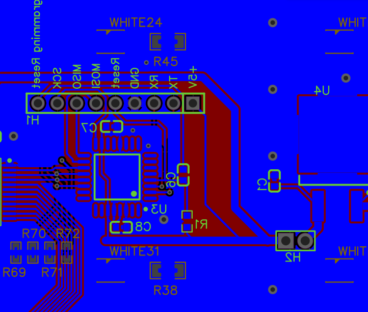
I'm using MiniCore with the following settings to upload to the chip (Ctrl + U) also tried (Ctrl + Shift + U):
I've succesfully uploaded sketches using the same FTDI breakout and connector to a DIP style ATMEGA (as found on the Uno) on a stripboard.
Therefore, I suspect there must be something wrong with the way I've set up the chip on my PCB compared to my soldered stripboard.
Does anyone have any ideas what I might be doing wrong? The only idea I have at the moment is that I've connected the two VCC and GNDs with the same capacitor. But then, this did not cause problems with bootloading.
FYI I use the Programming reset connected to the DTR pin of the FTDI connector.
After doing some more research, the only thing that I've been able to discern is that the tolerance on the internal crystal of the -AU version might not be tight enough to allow for programming properly?
Hi jremington, thanks for the information. I've read through some of the datasheet regarding the oscillator. It's very complex and I imagine this means tweaking the bootloader settings in the MiniCore library?
Looking into the MiniCore library more because of this and your suggestion, it looks like they have a few suggestions for the problem I'm facing:
No, it means calibrating the internal oscillator (OSCCAL register) against some reference, so that its frequency is closer to 8 MHz. Although that won't solve the problem, if it is due to faulty PCB design and construction.
In any case, if you want to succeed in projects like this, at some point you really must learn to read and understand the data sheet.
I happen to use a 32 kHz watch crystal on PB6 and 7 (plus 2x30 pF crystal load capacitors), driving Timer2 for oscillator calibration, and this code, which originally came from an Atmel application note:
//
// Calibrate the internal OSCCAL byte, using the external 32768 Hz crystal as reference.
//

void OSCCAL_calibrate(void)  //This version specific to ATmegaXX8 (tested with ATmega328)

{
  unsigned char calibrate = 0; //FALSE;
  unsigned int temp;

  TIMSK1 = 0; //disable Timer1,2 interrupts
  TIMSK2 = 0;

  ASSR = (1 << AS2);      //select asynchronous operation of timer2 (32,768 Hz)
  OCR2A = 200;            // set timer2 compare value
  TCCR1A = 0;
  TCCR1B = (1 << CS11);   // start timer1 with prescaler 8
  TCCR2A = 0;
  TCCR2B = (1 << CS20);   // start timer2 with no prescaling (ATmega169 use TCCR2A!)

  while (ASSR & ((1 << TCN2UB) | (1 << TCR2BUB))); //wait for TCN2UB and TCR2BUB to be cleared

  delay(5000); //5 seconds to allow 32 kHz xtal osc to stabilize

  while (!calibrate)
  {
    cli(); // disable global interrupts

    TIFR1 = 0xFF;   // clear TIFR1 flags
    TIFR2 = 0xFF;   // clear TIFR2 flags

    TCNT1 = 0;      // clear timer1 counter
    TCNT2 = 0;      // clear timer2 counter

    while ( !(TIFR2 & (1 << OCF2A)) ); // wait for timer2 compareflag

    TCCR1B = 0; // stop timer1

    sei(); // enable global interrupts

    if ( (TIFR1 & (1 << TOV1)) ) temp = 0xFFFF; //overflow, load max
    else   temp = TCNT1;

    if (temp > 6150)  //expect about (1e6/32768)*201 = 6134 ticks
    {
      OSCCAL--;   //RC oscillator runs too fast, decrease OSCCAL
    }
    else if (temp < 6120)
    {
      OSCCAL++;   //RC oscillator runs too slow, increase OSCCAL
    }
    else calibrate = 1; //done

    TCCR1B = (1 << CS11); // (re)start timer1

  } //end while(!calibrate)
} //return
If you do, configure the chip to output the internal oscillator, get the scope or a frequency counter out and determine the actual oscillator frequency.
When you upload the bootloader, you must have previously selected the correct board / clock speed since the bootloader is selected specifically for the chosen combination.
That if a bootloader is installed and later a sketch is uploaded using the programmer over the ICSP header, the bootloader is overwritten and must be re-installed for any later attempts to upload via a USB/Uart (FTDI) adaptor.
That, when you do use a USB/Uart adaptor to upload a sketch, the TX and RX lines are normally crossed. However, with one exception. That is, when an Arduino has been configured as a USB/Uart adaptor and the reason is the that TX and RX markings on the Arduino board refer to its ATmegaXX chip and not the onboard USB/Uart adaptor (which you are interested in in this case).
So, it seems like you and Sading were correct. Reversing the TX and RX lines resulted in a successful upload.
Can you elaborate on point 3 that you made. I'm struggling to understand why this worked if I've matched the pinout from the chip to the pinout on the FTDI connector?
Are you using a purpose built FTDI adaptor or are you using an Arduino in the role of an FTDI adaptor ?
Normally, if you connect a FTDI type adapter to an MCU, as an example, you connect the pin labelled RX on the FTDI adaptor to the pin labelled TX on the MCU. That is, these are crossed over. That is because something which is being transmitted from the TX pin of the FTDI logically must be received on the RX pin of the MCU. Or is it the exception to this rule, when using an Arduino in the role of an FTDI adaptor, that you are having trouble with ?