ATtiny85 check circuit

Hi,
The project is that the Attiny85 receives from the JDY-08 (that is connected via bluetooth with my smartphone) some data, and then the attiny85 act like a keyboard and mouse that write on the pc something, like for example the data. The problem is not the coding.
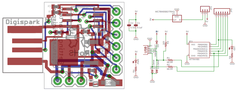
So I have done this circuit that is powered from the USB 5v of a PC:

and this is the pcb:


Do you thing is all right? the circuit I think is ok.
Just to be sure before print it. The only question is if this is gonna work like kayboard and mouse.

Have You verified the function? Built a prototype?

No, never. Looking at Your pictures is way too little.

Ask the spirits.

Dry reading code, even schematics and especially PCB pictures like that needs the powers of God to be sure.

Can't be, because D1 is the wrong way round.

You forgot the voltage divider on the RX pin of the BT module.
Now you're feeding 5volt-logic into a 3.3volt pin.
That might be ok for a while, but...
Leo..

So if I convert everything to 3.3v with the AMS1117 and connect the Attiny85 and JDY-08 to the Vout of the AMS1117, it should not be a problem for the feeding 5volt logic to 3.3v pin.

I do not understand, do you mean the the Rx and Tx are reversed? Or that I have to connect the Tx to the A1?

1 Like

What are you asking for help with?

If the circuit is ok. But I have understood that I have to convert everything to 3.3 volt.

But i dont understan what mean "Can't be, because D1 is the wrong way round"

No.
If you do, then you have problems with feeding the 5volt USB data signals into the Attiny.
Just leave the Attiny powered from 5volt, and add a 1k:2k2 voltage divider to the RX pin of the BT module. Lots of examples for that on Google images for HC-05 modules.

Diode D1 is pointing towards the USB connector, which is wrong. Turn it around.
Leo..

a1b168767a48a278e16768a01f2b5ac66161727fEC

This is the correct orientation for D1.

Do you now see what was meant by "D1 is the wrong way round" ?

Ooooo sorry I was thinking about the Attiny85 sorry sorry. Thanks.

Ok thanks, sorry again. I will do it and I will post the new circuit when done.

PB3 - USB+ -> D+
PB4 - USB- -> D-
Ok?

But, I don't find nobody with this.
I only find people saying PB4 to D+ and PB3 to D-.

So I think this will be ok?

But ua6em showed you a commercial product in post #5, with PB3 connected to D+

I still do not understand, where are connected the PB4 and PB3?

Even watching this image : https://ericdraken.com/files/attiny85-schematics.png

But i'm getting confused, becuase the image that @ua6em posted say how you say, the PB3 connected to D+...

Now i'm very confused.

But I decided anyway to update the pcb (PB3 to D+ and PB4 to D-):

And it is right! At least one of the reloaders can be used :wink:

Ok thanks very very much all here.
I will print this the last schematic I posted!

Hi again everybody. It's been a month, and finally i could get the pcb printed, and now finished to solder.
The problem is that when I plug it in the PC, my PC say that have been plugged a usb that could not be recognized, and i can hear the sound of usb plugged in, but I don't hear the sound of unplugging usb (good?).
So I can't use the Digispark Uploader to upload.
What I have to do? the Attiny85 is unsoldered from a working Digispark Attiny85 board.
Screenshot of the error (found on internet becuase I have windows in italian)

I have to install the Micronucleus Bootloader? but if i do that will I be able to upload sketch via USB?

There is a special way of uploading sketches to the digispark, with the Micronucleus bootloader.

It is detailed at: http://digistump.com/wiki/digispark/tutorials/connecting

I found the problem, sorry for wasting your time.
The PB3 and PB4 are inverted...
they must be:
D+ -> PB4
D- -> PB3

NOT:
D+ -> PB3
D- -> PB4