There is a solution to your problem and it is very simple ( though the description is a bit long winded).
Lets assume you are using an N channel Mosfet. In order to minimize power dissipation, you correctly assume that you must switch the FET on and off as fast as you can. As well as that you must select a device with a very low on resistance 1 to 2 milli ohms would be ideal. A high voltage FET is not required 30 to 40 V is adequate.
The switching frequency of 500Hz is probably adequate as the process relies on the thermal inertia of incandescent lamps.
To ensure that your FET is fully enhanced (switched hard on) with a 12V supply, a Logic level device is preferable. These are designed to be fully enhanced with the Gate / Source junction at 5V and will most certainly be so at the 10 - 12V you are likely to achieve.
I had a rummage on the Farnell web site and came up with an IRLB3034 which is a 40V N channel part rated at 195A and 1.4 milli ohm
The Gate / Source junction of a MOSFET is essentially capacitive and to switch the device on quickly this capacitance must be charged up quickly. To achieve this, resistors / resistance are you enemy.
It is worth noting that whilst charging the Gate / Source capacitance requires a substantial current it is only a very narrow pulse. I measured it in simulation at 300mA.
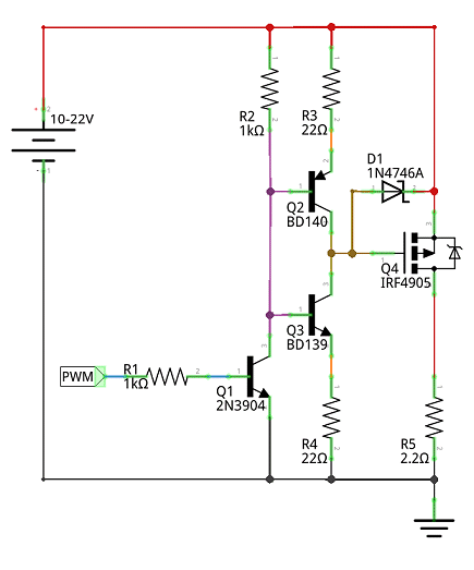
The accepted way of switching MOSFETS quickly is with a 2 transistor totem pole arrangement which will alternately charge and discharge the Gate / Source capacitor very quickly. The method is applicable to both N and P devices. Hopefully my picture will be attached (this is my first attempt, and if not perhaps someone will explain how) and will show the simple arrangement of totem pole Q1 and Q2 driving Mosfet Q3. The voltage source is the output of your Arduino.
I have used this circuit many times and have just designed a 15A buck converter (using a P channel device) running at 280KHz and no problems with stability. The transistors I use are rated at 45V will switch 800mA have a gain of 170 and fT (where gain reduces to unity) of 100MHz.
To keep the whole thing stable, the output of the totem pole must be connected directly to the gate of your device with the bottom end of it connected directly to the source. Don't be tempted to put a resistor in the gate connection. One of the main reasons for instability of these types of circuit is the inductance of wiring and long PCB tracks plus inadequate de-coupling of power supplies. You should also connect a large capacitor 100uF or so at the PSU input and connect others at supply pins for other devices.
Also, and very important, you must connect all the high current ground parts of your circuit including the PSU ground at a single point, do not daisy chain.
A further requirement for keeping the circuit stable is to keep all the wires as short as practicable and keeping the output wiring away from the drive circuit of the FET to avoid inductive or capacitive coupling.
To summarise. Whilst the rise fall time of the FET gate drive will have some effect on power dissipation these periods are relatively small compared to the on period. The bulk of the power dissipation is a result of the on resistance of your FET so you must ensure that your selected part is fully enhanced.
Hope this helps!
Totem pole.pdf (10.4 KB)