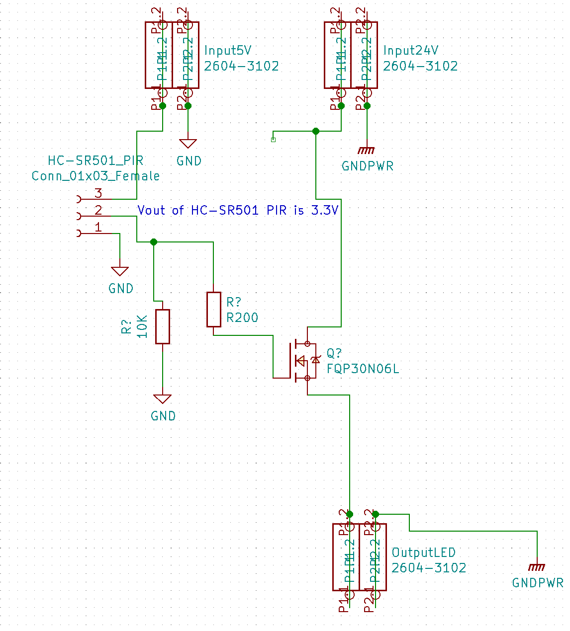
I have an HC-SR501 sensor that I use to turn lights on and off. The HC-SR501 is powered by 5V, while the LED is powered by a 24V 800mA LED driver. They have separate grounds.
Up until now, the HC-SR501 was directly connected to a 30N06L MOSFET on a board that includes a 10k pull-down resistor. There was nothing else between the HC-SR501 and the MOSFET. This setup worked okay, but some of the HC-SR501 sensors broke down after a while (1-3 years). This could be due to a quality issue or my poor circuit design.
The more I read about MOSFETs, the worse this setup seems.
I am currently changing it a bit. At the very least, I think I need to add a resistor between the gate and the output pin of the sensor (see schematic).
However, looking at the specs of the MOSFET, 3.3V and 0.8A are hard on the limit. This implies that I need to use another MOSFET or a MOSFET driver. Furthermore, I assume that a proper design would use the same ground or need an optocoupler.
This is a hobby project, and I would like to stick to through-hole technology (THT) or somewhat easy-to-solder options.
Questions:
Do you think the proposed schematic should work reliably?
Are there any simple improvements you would recommend? A better MOSFET? A logic level Mosfer?
Do I need to go with a MOSFET driver (and optocoupler)?
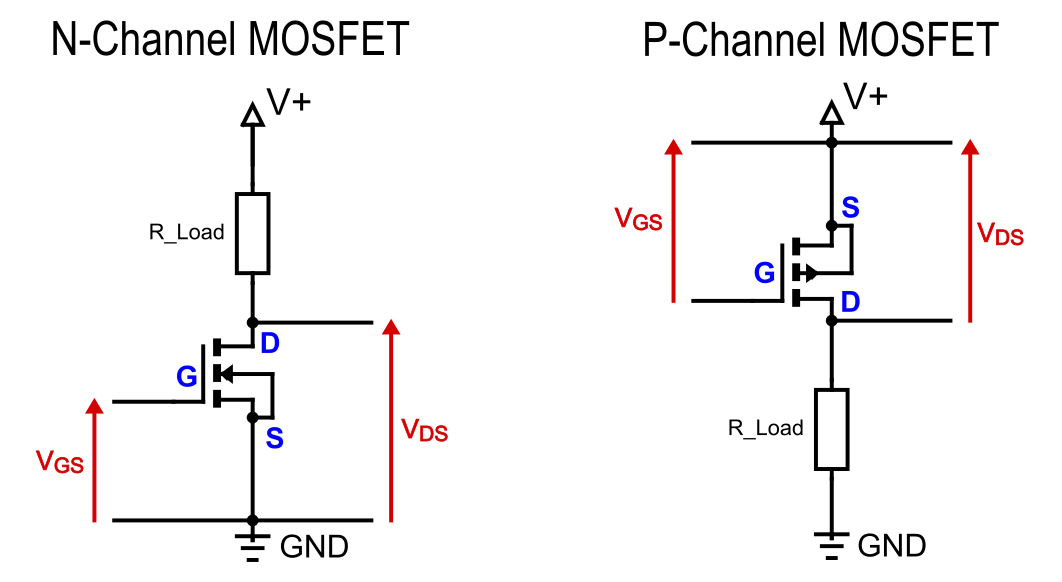
I have difficulties interpreting your schematic but, in principle, if you are using an N channel mosfet to power something, then the mosfet switches on the low side. That is, the power source positive is connected to the devices to be powered, LEDs in your case, and the LEDs are connected to ground via the mosfet.
Especially regarding the flaw in the position of the Load.
I'd rather isolate them from each other with an optocoupler.
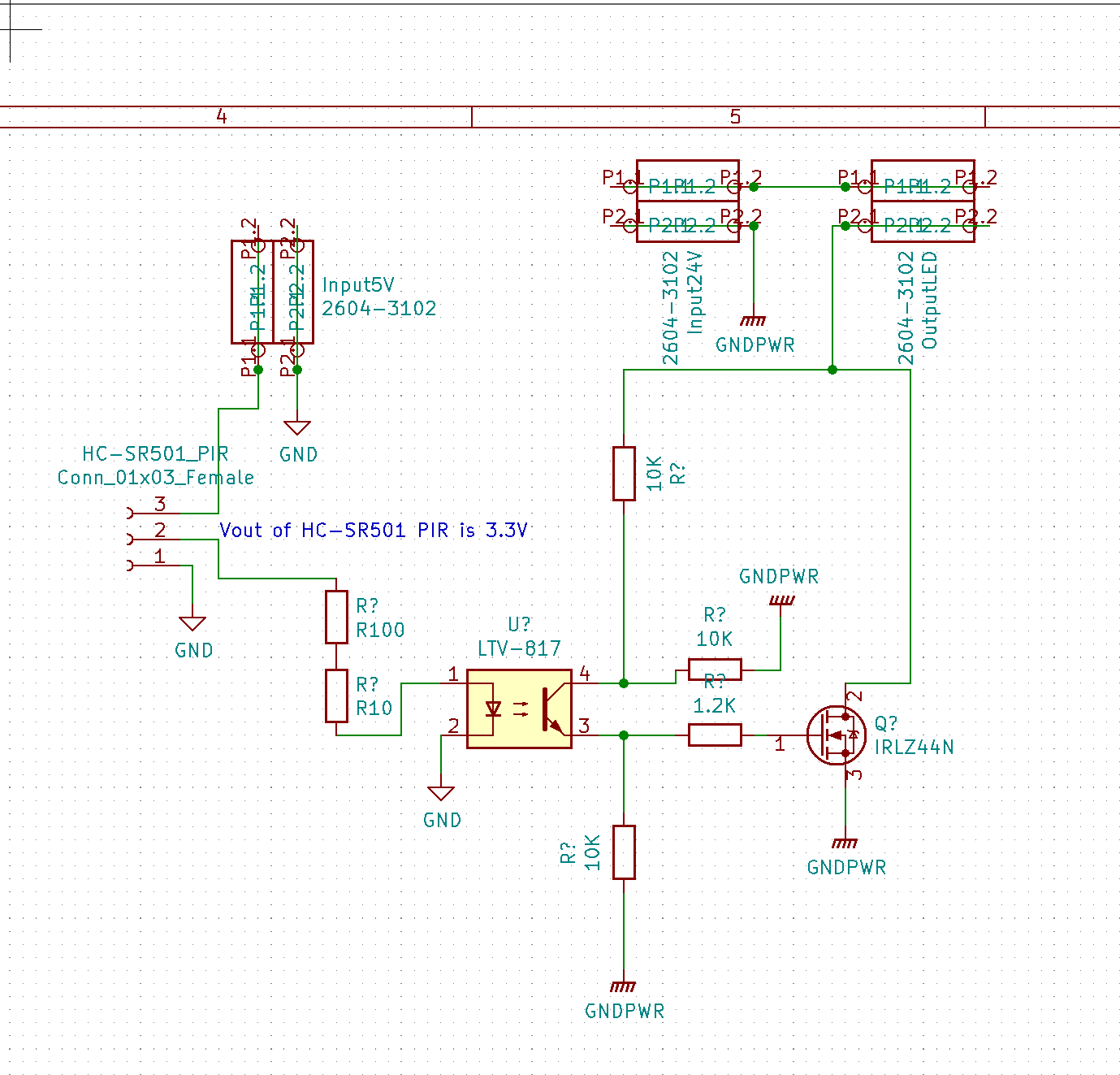
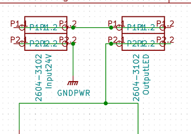
I have updated the schematic. Also regarding the mentioned flaw. The load would be connected at the OutputLED Connector.
There is a voltage divider to prevent a too high voltage at the gate.
I limited the current for switching the gate to 10mA (1.2k/12V).
To my understanding, this could lead to a bit slower switching. For this application (no PWM), this shouldn't be an issue. (I hope).
Like that, I assume, that I won't need to add a BJT or a driver.
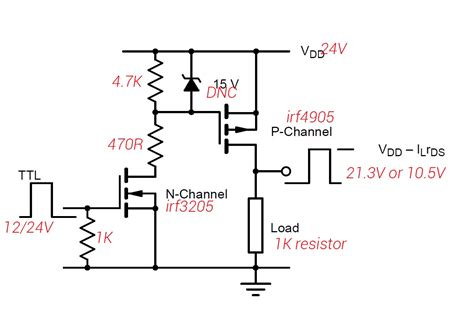
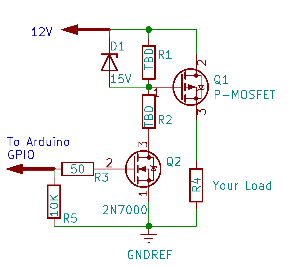
This setup is designed for 24V but works just fine on 12V. If you’re powering it with a processor, change the 1k resistor to 10k and connect it to the port pin. Add a resistor in the range of 50 ohms between the port pin and the MOSFET gate.
The 15V Zener diode is crucial if there’s a chance of power supply spikes. It protects the MOSFET gate from over voltage. While the circuit will work without it, I always recommend including it for added protection.
Can you explain these schematic symbols. They are not conventional. You appear to be using a similar symbol for both a power source and a load and it is confusing.
Thanks for your answer. The 2604-3104 are both Wago Terminals on the PCB. Both, the load and the PSU are external. Of course, you are right. Replacing the Wago Terminals would increase the readability in this context.
Please, let me ask some questions for clarification.
To prevent a common ground, could I replace IRF3205 with a optocoupler?
Is there a reason to use a P-Channel over a N-Channel? (Other than the wrong load position in my first sketch?)
On the schematic, it seems that a TTL of 12/24V is assumed. In this case, Vgs could be reached without any issues with the TTL Voltage of 12/24 V. And only one Mosfet would likely be necessary. My main issue is, that TTL will be 3.3V at max. Did I miss-read the schema?
R1 turns the MOSFET off. R2 may not be needed, depends if you use voltages above 12V. If so adjust the ratio to get about -12V on the gate when Q2 is on. This voltage is in reference to the 12V (source) not ground. R3 softens the surge the Arduino pin will see because of the gata capacitance. R4 is your load R5 guarantees that it will be off unless the Arduino is driving it. Q1 is your P-Channel MOSFET that switches your load represented by R4 Q2 forms an inversion and a level shift as the gate needs to be at +12 to be off. Note This ground reference must be connected to the Arduino ground.
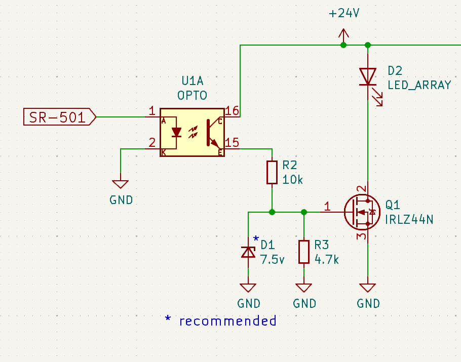
The SR-501 has a 3.3v pushpull output via a 1k resistor according to this: https://www.mpja.com/download/31227sc.pdf . If this is the case, no series resistor is needed (wanted) for the optocoupler LED.
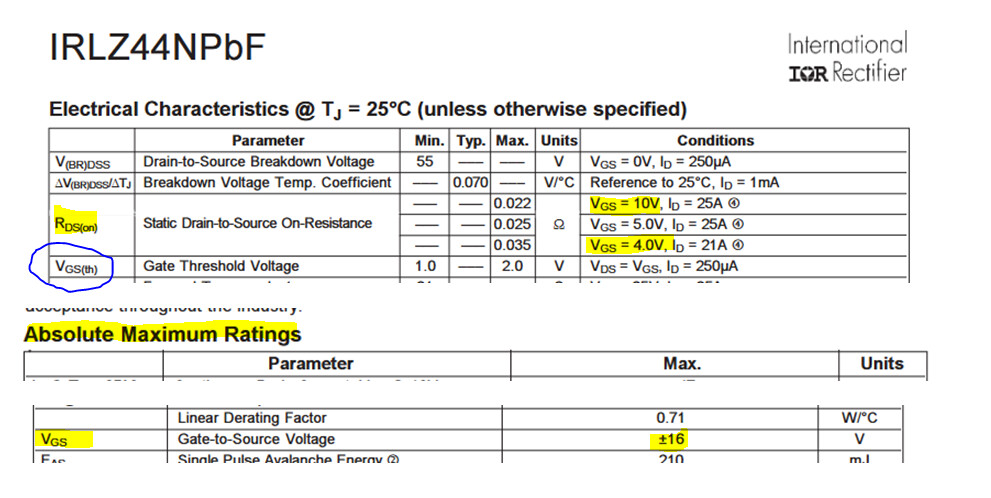
The IRLZ44 has a max Gate Source voltage (Vgs) of 10v
I guess I'd do it like this:
Just out of curiosity to improve my knowledge for the next project.
Is there a rational to limit Gate Source to 7.5 V? The IRL would be rated to 16V. Thus limiting Vgs to 12 V should be sufficient? Or is it best practice to have a safety factor of two in place?
I based the circuit (post #11) on your post #4 where you are using the IRLZ44N (N channel mosfet) in a low side switch configuration. The other circuits which appeared here are in a high side switch configuration with a P channel mosfet.
However, you could also modify the circuit to cap the Vgs at 10v instead of 7.5v. Change the Zener diode to 10v and R3 to 8.1K. This would also work equally well with both the IRLZ44N and the FQP30N06L. It is important not to exceed the Vgs(max) and even short spikes above this value can destroy the device, hence the caution. As a guide, you can aim for the Vgs at which the lowest Rds(on) is quoted, in this case 10v. If that is not possible ensure you do not go below the Vgs at which the highest Rds(on) is quoted unless you know what you are doing. The Vgs(th) is really only useful for knowing when the mosfet if fully off.