CrossRoads, ive had a bit more time to go over the picture you last uploaded. Can we put in a hole for pins:
next to the servo pins for power and ground.
Ground for POT, i see you have already powered it
power and ground for the LSM303
move all the ones marked header/serial next to each other and add power and ground in and 8x2 row. ( i use a USB header cable to connect to an arduino for programming.)
can we add a 7809 for 9v power so it can be powered off 12v and still supply both 9 and 5 volts?
other questions:
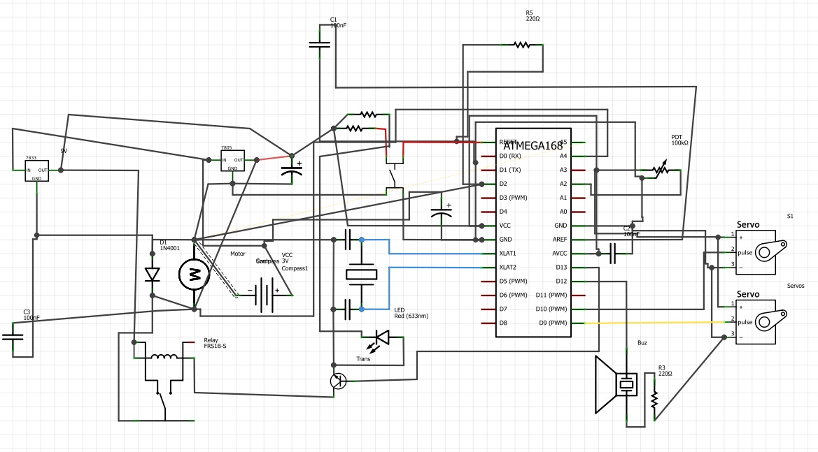
what is it you have put on the aref and avcc that goes to ground?
what is it on A6 that goes to power? i see a resistor and something else. and i dont see where it connects to the header.
thanks heaps for doing this btw theres no way i could knock that up as fast as you did.
Sure, your changes are all minor. Don't know if staying single sided will still be possible. Have to see how slow the Olympics are going
You can print the layout as is, the chip and header holes are 0.1" apart.
Pot has 3 pin header for power, wiper, gnd.
Aref has cap to gnd only, does not connect to 5V - that's taken care of internally.
VCC/AVCC get 5V and a cap to gnd.
I don't know what you mean by A6. Looked to me like the Reset pin.
The switch, folks typically use internal pullup and connect the pin to ground with the switch, vs connecting the switch to +5. I wired it like you drew it tho.
sure man, in your own time. i cant complain about free support.
Pot has 3 pin header for power, wiper, gnd.
ok, i see that now.
Aref has cap to gnd only, does not connect to 5V - that's taken care of internally.
VCC/AVCC get 5V and a cap to gnd.
thanks, understood.
I don't know what you mean by A6
sorry, a6= rst. its labeled as a6 on all the chips ive bought.
I wired it like you drew it tho.
i may have drawn it wrong, and possible soldered it all together wrong. its meant to be just a reset switch. and be part of the header (8 pins)
rst, D0, D1, D13, D12, D11, gnd, 5v (think i may have missed 12 previously.)
basically i copied this:
So you really want an ICSP header (D11,12,13, +5, Gnd, Reset) and an USB/Serial adapter header (Rx, Tx, DTR, +5, Gnd, and typically a 2nd Gnd; FTDI chip needs it to pull its CTS (clear to send) input pin low.
CrossRoads:
So you really want an ICSP header (D11,12,13, +5, Gnd, Reset) and an USB/Serial adapter header (Rx, Tx, DTR, +5, Gnd, and typically a 2nd Gnd; FTDI chip needs it to pull its CTS (clear to send) input pin low.
6: Rx, Tx, DTR, +5, Gnd, and a 2nd Gnd which is actually CTS input to FTDI chip.
Or use CP2102 module, then only 1 Gnd. Have to modify the board to connect CP2012's DTR output to a pin instead of CP2102's Reset input (cut a trace, add a wire).
Hi, I'm
Happy just to use another arduino, rather than the cp2102. But if it's too much trouble, don't worry about it, I can always take the chip out to reprogram it. It's just easier not to.
The servos I'm using plug goes signal, power ground.
Would it make it easier to stay single sided if you added holes for small jumpers instead of changing sides when you can't cross another wire?
Ok, just a thought. Stick with whats easier. if you cant add the header, then dont worry. i think i would be able to get a double sided board if needed, but for being easier's sake, i think single sided might be the go.
itll be great if someone who has done this before can tell me where ive screwed up. i dont know i have for sure, but it highly improbable taht ild get it right on my first attempt
its a bit had, the schematic the program generates is a mess. and it going to be wrong, as ive been working on the pcb and just making it fit.here it is with labels. hope that helps.
No, that's not a schematic.
You also appear to be daisychaining the ground along. Suggest using a Ground plane let everything to be grounded connect to it.
Connecting the lower right signals to Gnd THRU the reset switch and on to half the board is not a good design.
I can see you don't have any 0.1uF decoupling caps on VCC, AVCC, AREF pins so you will also have erratic operation.
I think your LED is also flipped around.
Those kind of things would be readily apparent on a schematic.
You also appear to have Aref connect to Vcc, I believe I have mentioned not to do that, to just use a 0.1uF cap from Aref pin to Gnd.
I Have made the changes you suggested, but still the schematic this program has generated for me is a mess.
you can see that not much is apparent from the schematic but i can see things are wrong with it that are right on the board.
as for the LED, i think your right, but it has the square hole connected to ground and round to power (like all the other parts) its the silkscreen picture thats ares about it recon.