Sounds like what you are saying is even though they are already on the Nano a second set wouldn't hurt.
That sounds more like what I'm used to seeing. GND expanded to a plane? Im not sure what that means but I have seen other boards where the bottom surface looks like its 80% ground. As in they expand the width of the traces in some areas. I don't know if I can figure out how to do that in my free version of the Eagle Cad software.
That actually sounds really good. For one I had no idea of how I was going to solder the stand off pins to the board. Bottom should be a lot easier.
Draw a polygon on bottom (and top) completely around the board, and then name them "GND" (or whatever matches the signal name you've given your GND connection...)
Here, the big red and blue rectangles just outside the board outline are GND Polygons. The next time you do a "Ratsnest" command, they get filled in as much as possible...
Yes, although I would put a 10uF and a 0.1uF across the 5V.
A protection diode in the 13.8V to protect against reverse polarity connection.
As for track widths, the PCB manufacturer should have on their site the answer to track widths.
As I said before, track width also helps the physical stability of any solder termination.
That DC-DC converter should be fine, especially as its input is up to 24V tolerant.
You may be better to mount the DC-DC converter separately, so 13.8 V does not get into the PCB, which will help with any vehicle noise.
Your layout is good, in that the thermistor part is in an area away from the output components.
My philosophy on PCBs.
I buy a blank PCB, fully loaded with copper.
I am going to pay someone to remove that copper, I don't get a discount for copper removed.
So I would like to keep as much of the copper, that I purchased on my PCB as possible.
I would at least double and where possible triple the width that you have.
Use a company to just make the PCB from your PCB file , you can’t just remove the copper from a plain board as you won’t have connections between top and bottom layers or plated through holes
The challenge is coming down to space. This car not only has a V12 engine packed into the space of a V8. It also has V12 fuel injection computers ( two 6 cyl ECU's) packed under the dash. I think I can design a cover to hold the 5V Buck converter just above the board without increasing the depth more than 1/4".
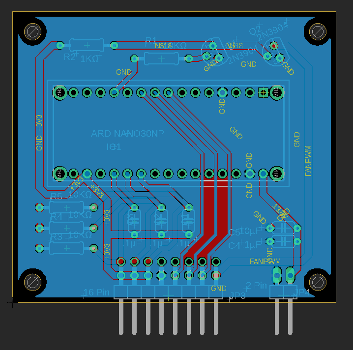
This is what I have so far. The buck converter will be off the board and connected to the input pins. I had to totally recreate the board because I had a fight with the software and it just had to be deleted and I had to start all over. A lot of work left to do on the board.
Hi,
Looks good, the gnd that goes from your two BJT emitters, would be better going from the emitters directly to the gnd point at the gnd connector pin on JP4.
In fact the gnd of JP4 needs to go somewhere.
The trace could go on the RED side of the PCB.
If you are going to use a DC-DC converyer to 5V, the positive of J4 will need to go to the 5V pin on the Nano not Vin.
OK I inadvertently deleted the ground in the schematic.
I rewired the ground to the two transistors. I set the trace sizes to 50, 32 and 20 mils. 20 is the largest that will fit between the pins.
The plan is to take the JP4 two pin connector out and just solder in two wires that come from the DC-DC converter.
So now I am having trouble figuring out how to edit this board after running the rats nest in Eagle software. Once I run the rats nest, I get the what is shown in pictures 3 and 4 for the top and bottom layers. I cannot undo these or find anyway to get back to the second picture where I can edit stuff.
You have big thick traces running perhaps-overly close to pins for no good reason.
You should probably do a "change isolate" on your ground polygons to make them back off a little from the other traces. Otherwise they'll use the default "minimum clearance" for the board (which is probably the 6mil number that we've already complained about.)
That's easily fixable in those areas. I was assuming if the software didn't flag it it was good. I'm a little more concerned about areas like this where there is not much I can do. I can easily give some clearance to the red trace but those blue are about the best I can come up with. The area of concern you highlighted are using 50 mil traces. Should those be thinned out to maybe 40 or 32.
The blue traces shown in the attached picture are 20mil. But they only carry enough current to drive an LED. And now that I think of it I should probably put a resistor in those traces.
I believe these are the settings you refer to. Looks like the spacing is 50 and not select-able. I currently have isolate at 0 and it can be set from 0 to 254. The polygon pour is set to solid, the other options are hatched and cutout.
I set Isolate to 16.
I also had to add three resistors for the LED outputs.
I re-routed wires using vias to get all the wires that would be difficult to solder on the bottom.