Not sure where to post but thought I would start here. Looking to direct solder an Arduino Nano Every to a carrier board but can't find a proper footprint to use in my design. Any idea where I can find the proper pad size and spacing for using the castellated pins? I'm unable to request support directly from Arduino. Any help would be appreciated. Thanks!
The Every has holes also - why not just use pin headers to connect it to perf board or whatever you are using?
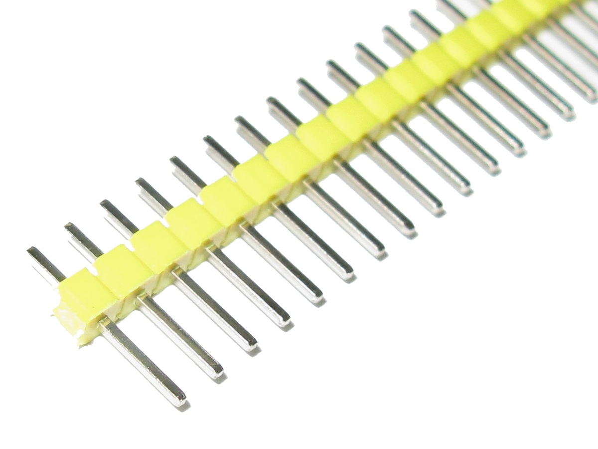
Example
http://www.dipmicro.com/store/HDR40T-Y
I'm trying to get the lowest possible profile as the spacing is tight with my prototype so I'd prefer to use the castellated pins vs regular header pins.
Sorry, I don't know of a 30 pin, 0.6" width breakout board like that.
Can you just use pins thru the Every and the perfboard without using the plastic housing that keeps the pins lined up?
Discrete pins,
https://www.digikey.com/en/products/filter/terminals-pc-pin-single-post-connectors/323?s=N4IgjCBcpgbAnABiqAxlAZgQwDYGcBTAGhAHsoBtEAVgBZqAmEAXRIAcAXKEAZQ4CcAlgDsA5iAC%2BJMPAAc8FCHSRs%2BYmUohkrEJ258hYySQC0TaEqgCAruvKQq1ECQXMpIEwovKbdzRDd3cyo2ETwWElhFQQATbhMwRAh2LkgQZxAOAE82Am4sPHQJCSA
Or break up a strip of pins and cut them short after soldering them in.
I'm not using a breakout board, I'm designing the carrier board myself, but am unable to find the proper footprint to use for it.
Ah! Then it sounds like you need to make a symbol for the Every.
Which CAD program are you using?
There is info here
https://store.arduino.cc/usa/nano-every

Yes I've reviewed those files already. None of them carry a footprint for the device. I already have a symbol and a 3D model. I just need the proper footprint now. I'm using Altium for my board design.
Sorry, I don't know Altium for designing electrical and footprint symbols. Have never used it.
I normally construct board “footprints” by starting with the board and deleting all the components that aren’t off-board connectors.
It may be difficult with the castellations, since the footprints don’t match the pads, and they’re frequently made (afaik) by letting the board edge slice through normal pads...
Measure or look up the castellated "pin" pitch.
See if it matches any of the small outline chip formats.
Find an adapter to match the pitch.
An example I use.
XBee Series three modules come in several formats including a surface mount version.
A 32 way TSSOP adapter (eBay) is a good match.
I cut it in half length-ways to match the XBee width.
The XBee has "pins" on three sides. For the horizontal pins, I simply use wire wrap wire to link the pins to the adapter.
Digikey do a lot of adapters and did do one for the XBee, then stopped. Hence the TSSOP solution.
If I had time, I would do a proper adaptor, but for just a few, it's not worth it.
@tigger, you're missing the gist of the question, see reply # 5.
@placebo0311 is using Altium to design a board, he needs the symbols for the Nano Every, which has 15 pins, 0.1" pitch, centers spaced at 0.6".
I don't think he knows how to create symbols in Altium.
It'd be a breeze for me to do in Eagle, something like this perhaps, or perhaps with the pads not extending quite so far out.


Crossroads, I'm always missing the point.
Mine was just a non-PCB solution.
I can see your layout is just like the adapter boards I use.
In fact the longer pads are a bonus when I chop it down the middle, as it gives a bit of leeway.
In any case, I always like to do a rough prototype.
I know how to make symbols in Altium, not sure where you got that assumption. Again though the symbol isn't the problem. I'm trying to make sure I use the correct pad size for castellation in order to ensure a good connection. I was hoping maybe there might be a standard of sorts for pad size. Since these use standard .1" pitch headers, the spacing is known, but wanted to verify the correct pad dimensions. It appears there is no standard and I'll just have to come up with something via trial and error. Appreciate the help nonetheless though, thank you.

Very good, I can work with that, thank you. Just so I'm clear and not misunderstanding, your units are in mils correct? So the pads on the Nano are 60 mils wide and 120 mils long for example, yes?
Yes, good catch, 60 mil x 120 mil, 0.06" x 0.12". Had my units a little off there. 0.6" x 1.2" would be huge! Don’t know how I missed that when I proof read it.